Research on a Fully Domestically Produced RapidIO Solution Based on Loongson 2K1000 Processor and Fudan Micro FPGA K7
After more than 20 years of development, the RapidIO bus protocol [1] has become one of the preferred solutions for high-performance system interconnects [2] based on packet switching. It is widely used in various fields such as wireless communication, military, supercomputing, medical image processing, and industrial control, all of which are, without exception, related to the national economy, people's livelihood, and national security. Currently, chips providing RapidIO bus interfaces mainly come from NXP's PowerPC (from the US), Texas Instruments' C6000 series DSP, Renesas' TSI series RapidIO switch chips and PCIe-to-RapidIO bridge chips, as well as Xilinx's RapidIO IP soft core. Domestically, there are few localized alternative solutions comparable to the aforementioned chips.
This article proposes a fully domestically produced RapidIO solution based on the Loongson 2K1000 processor [3] and Fudan Micro FPGA, and verifies the feasibility of this solution through a specific project.
1 Solution Design
1.1 Overall Design
Complex embedded devices, such as core network high-end switches, routers, 5G base stations, and aircraft avionics systems, generally adopt a multi-daughterboard rack-mount design. These daughterboards are interconnected by signals routed through the backplane, thereby achieving communication between them. Communication between daughterboards generally includes data plane communication and control plane communication. Data plane communication typically requires high-reliability, high-bandwidth, low-latency full-duplex communication. Corresponding data plane system interconnect solutions include RapidIO bus, Ethernet, and PCIe bus, among others. The RapidIO bus, with its advantages of high transmission bandwidth, fewer interconnect signal lines, strong anti-interference capability, and ease of expansion, has become the preferred high-speed interconnect solution for daughterboard data planes in complex systems such as aircraft avionics systems.
The Loongson 2K1000 processor (hereinafter referred to as CPU) is an embedded SoC processor developed by the Institute of Computing Technology, Chinese Academy of Sciences, targeting network applications, industrial control, and other fields. It integrates two 64-bit dual-issue superscalar GS264 processor cores on-chip, compatible with the MIPS64 architecture, with a main frequency of 1 GHz. It also integrates various peripherals such as a 64-bit DDR3 controller, SATA3 controller, two x4 PCIe 2.0 controllers, and two Gigabit Ethernet controllers. The Loongson 2K1000 processor has rich peripheral resources, making it suitable as a processor for control daughterboards. However, since it does not integrate a RapidIO controller on-chip, a more feasible alternative is to use a Fudan Micro JFM7K325T FPGA with a RapidIO IP soft core to implement the RapidIO bus interface, and then select the PCIe 2.0 bus interface as the data path between the Loongson 2K1000 processor and the Fudan Micro FPGA. The RapidIO bus on the FPGA side uses an LP-Serial x1 physical layer interface, operating at a frequency of 3.125 GHz, with a data bandwidth of 2.5 Gb/s. In terms of software, the domestically produced Reah real-time operating system runs on the Loongson 2K1000 processor, and PCIe drivers and RapidIO drivers under the Reah system are developed. In terms of hardware, a domestically developed RapidIO IP soft core from AVIC General is used. A minimum subsystem is built with the Loongson 2K1000 processor and Fudan Micro JFM7K325T FPGA as the core. The overall system design [4] is shown in Figure 1.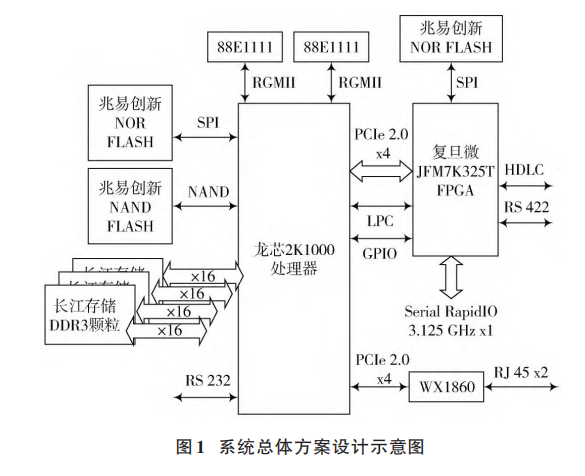
The CPU and FPGA are connected via PCIe bus and LPC bus, where high-speed signals are transmitted using the PCIe bus, and control signals are transmitted using the LPC bus. RapidIO differential signals are routed out from the FPGA. Both the CPU and FPGA use SPI bus-based NOR FLASH to store boot firmware. The CPU uses parallel Nand FLASH for large-capacity file storage. The CPU is externally connected to four x16 domestically produced DDR3 chips. The two on-chip integrated GMAC Ethernet controllers of the CPU are externally connected to 88E1111 Gigabit Ethernet PHYs via RGMII interfaces. In addition to routing out RapidIO signals from the FPGA, it also implements HDLC synchronous serial signals and RS-422 high-speed serial signals. All peripherals of the subsystem use domestically produced chips, such as FLASH chips developed by GigaDevice, DDR3 chips developed by Yangtze Memory Technologies Co. (YMTC), and 88E1111 Ethernet PHY chips developed by CETC 32nd Research Institute.
1.2 Data Transfer
There are two main ways for data exchange between FPGA and CPU via the PCIe bus [5]: PIO mode and DMA mode. The principle of PIO mode is that the FPGA allocates a certain range within the PCIe BAR space to implement data registers, control registers, and status registers. The CPU uses an MMU to map the PCIe BAR space and performs data exchange based on a simple data copy algorithm [6]. When using PIO mode for PCIe data transfer, each read or write operation to a data register by the CPU triggers a PCIe TLP (Transaction Layer Packet) transaction. When the data register is 4 B, the payload data only accounts for 4/256 of the TLP transaction packet. Coupled with the overhead of establishing each PCIe TLP transaction, it is easy to conclude that PIO mode is inefficient and thus unsuitable as a data path for a high-speed RapidIO bus.
DMA mode uses DMA channels in the FPGA to transfer data between CPU memory and FPGA memory. Each transfer aims to maximize the payload data within the TLP transaction packet, and the transfer process does not require CPU involvement. When the CPU sends data to the FPGA, the CPU only informs the FPGA of the address and length of the data to be sent, and the DMA channel is responsible for transferring the data. After the data transfer is complete, the FPGA notifies the CPU of the data transfer completion asynchronously via a PCIe MSI interrupt. When the CPU receives data from the FPGA, the CPU first informs the FPGA of the memory address where the data should be written. When the FPGA data is ready, the DMA channel transfers the data to that memory address and then sends a PCIe MSI interrupt to the CPU, notifying the CPU that the data transfer is complete. The CPU can obtain the actual length of the transferred data by reading specific FPGA registers.
This solution adopts an improved XDMA method [7], the core idea of which is to use a data descriptor linked list to control PCIe data transmission, reception, and synchronization between the CPU and FPGA. The XDMA data descriptor is shown in Figure 2. The length of the data descriptor is a fixed 32 B, and the buffer address storing the data descriptor must be aligned with the CPU cache line to ensure optimal memory throughput efficiency. The descriptor stores the length of the data to be transferred by the DMA channel, the source address of the data (used when transferring data from CPU to FPGA) / destination address (used when transferring data from FPGA to CPU). The control word field includes a data transfer completion flag bit, used to indicate the status of the data transfer. Descriptors are connected into a singly linked list via the "next adjacent descriptor address" field. This field is empty for the last descriptor in the list, serving as the end-of-list marker. The CPU prepares the data descriptor linked list as needed before receiving and sending data, and sets the address of the first descriptor in the list into the FPGA's XDMA register.
Sienovo provides Loongson + FPGA domestically produced solutions.