Power Applications Based on TI AM62X/AM64X + FPGA + AD7606/ADS8568 Multi-channel ADC Acquisition
Power Applications Based on TI AM62X/AM64X + FPGA + AD7606/ADS8568 Multi-channel ADC Acquisition
● Similar to asynchronous SRAM memory and dedicated ASIC devices.
● Asynchronous, synchronous, and page mode (only for non-multiplexed mode) burst NOR flash devices.
● NAND flash.
● ADC devices.
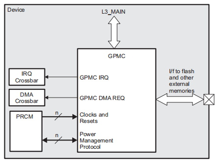
Figure 1 GPMC Overview
2 GPMC Parallel Interface Features
Why do industrial applications prefer using the GPMC interface when communicating with FPGAs/ADCs? This article provides 3 reasons: high bandwidth, rich connection modes, and flexible configuration. Specifically, they are as follows:
PS: The following will introduce an ARM + FPGA communication case based on AM570x GPMC, and a comprehensive multi-channel AD (AD7606/ADS8568) acquisition case.
(1) High Bandwidth, Speeds Exceeding 100MB/s
Taking AM57x as an example, when connecting to an FPGA via the GPMC interface and reading data from the FPGA side using DMA, speeds can reach 69MB/s. In fact, by configuring the GPMC interface's timing and different operating modes, speeds can exceed 100MB/s.
(2) Rich Connection Modes, Flexible 8-bit and 16-bit Asynchronous Memory Interfaces
Because the 16 gpmc_ad[15:0] pins support both address/data multiplexed and non-multiplexed modes, this makes the GPMC's connection modes with peripherals very rich, allowing communication with a wide range of external devices, such as:
● External asynchronous or synchronous 8-bit wide memory or devices (non-burst devices)
● External asynchronous or synchronous 16-bit wide memory or devices
● External 16-bit non-multiplexed NOR Flash devices
● External 16-bit address and data multiplexed NOR Flash devices
● External 8-bit and 16-bit NAND Flash devices
● External 16-bit pseudo-SRAM (pSRAM) devices
Several connection modes are introduced below.
- 16-bit Address /Data Multiplexed (Address and Data Line Multiplexed Mode)
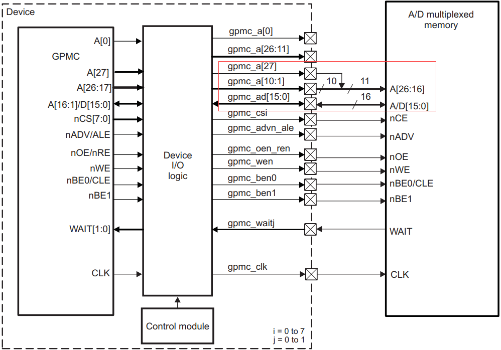
Figure 2
- 16-bit Nonmultiplexed (Address and Data Line Non-multiplexed Mode)
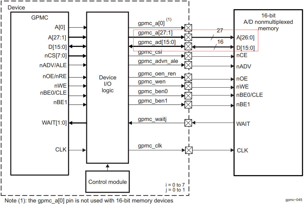
Figure 3
- 8-bit Nonmultiplexed (Address and Data Line Non-multiplexed Mode)

Figure 4
- 8-bit NAND (Data Line Only Mode)
This mode is suitable for scenarios where address lines are not required, such as GPMC connecting to NAND FLASH. NAND FLASH does not require address lines; read/write commands are sent via data lines D[x:0] for data reading/writing.
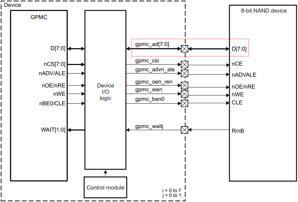
Figure 5
(3) Flexible Configuration, with up to 8 Chip Selects
The GPMC basic programming model provides maximum flexibility to support eight configurable chip selects with different timing parameters and bit width configurations. Optimal chip select settings can be used based on the characteristics of external devices.
● Different protocols can be selected to support general-purpose asynchronous or synchronous random access devices (NOR flash, SRAM) or specific NAND devices.
● Address and data buses can be multiplexed on the same external bus.
● Read and write accesses can be independently defined as asynchronous or synchronous.
● System requests (byte, 16-bit word, burst) are performed via single or multiple accesses. External device access profiles (single or multiple optimized burst lengths, native or emulated packets) are based on external device characteristics (supported protocol, bus width, data buffer size, native packet support).
● System burst read or write requests are synchronous bursts (multiple reads, or multiple writes). When burst or page mode is not supported by the external memory or ASIC device, system burst read or write requests are converted into continuous single synchronous or asynchronous accesses (single read, or single write). Only 8-bit wide devices are supported in single synchronous or single asynchronous read or write modes.
To emulate a programmable internal wait state, an external wait pin can be monitored to dynamically control external accesses during initiation (initial access time) and burst accesses.
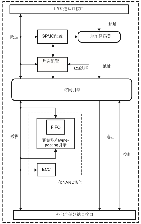
Figure 6 GPMC Block Diagram