Domestically Produced PCIe 4.0 Interface Signal Integrity Simulation Analysis, Taking 10 Gigabit Network Cards and 11-slot PCIe GPU Baseboards (PCIe 4.0/5.0) as Examples
PCIe 4.0 Interface Signal Integrity Simulation Analysis in 10 Gigabit Network Card Design
Given the current low accuracy and reliability of existing PCIe interface signal integrity simulations, a new PCIe 4.0 signal channel link model and simulation analysis method have been established. A ×4 PCIe 4.0 signal channel link model was built for a 10 Gigabit network card PCB using the simulation software POWERSI; time-domain, frequency-domain, and loopback simulations were performed in ADS software using the established model; and the simulated return loss, insertion loss, and eye diagrams were analyzed to determine if the PCIe 4.0 signal traces meet design requirements. The return loss for all 8 pairs of PCIe 4.0 differential signals obtained by this method was less than -6 dB, the insertion loss was greater than -28 dB, and the eye diagram's eye width and eye height were both greater than 0.3 UI and 15 mV, respectively, satisfying the requirements of the PCIe 4.0 protocol specification. Compared to existing simulation results, this method offers higher reliability.
The rapid development of integrated circuits has led to reduced signal rise times and increased clock frequencies, which in turn causes signal integrity issues. The severe consequence of this phenomenon is that circuits cannot function properly [1]. To eliminate this phenomenon, experts in relevant fields both domestically and internationally have dedicated themselves to researching signal integrity problems [2-7].
From PCIe 1.0 to the current PCIe 5.0, bus frequencies and transmission rates have multiplied, leading to signal integrity issues during signal transmission [8]. To address this problem, scholars both domestically and internationally have conducted a series of studies. Reference [9] used the simulation software Allegro Sigrity to perform time-domain analysis on PCIe 2.0 differential signals, obtaining their eye diagrams. The quality of PCIe 2.0 differential signals was judged based on the differences between input and output eye diagrams. The drawback of this simulation analysis method is that it only performs a simple time-domain analysis of PCIe differential signals, and there is no criterion for the tolerance range of differences between input and output eye diagrams, resulting in low reliability of the simulation results. Reference [10] used the simulation software Hyperlynx to perform time-domain and frequency-domain analysis on PCIe 2.0 signals, obtaining return loss, insertion loss, and eye diagrams. The PCIe signal quality was evaluated by comparing these with protocol specifications. While this simulation analysis method can effectively assess PCIe signal quality, it did not consider signal transmission over longer PCIe links, thus yielding results with limited reliability. Addressing the aforementioned issues, this paper proposes a new PCIe 4.0 signal integrity simulation analysis method. It establishes a ×4 PCIe 4.0 signal channel link model for a 10 Gigabit network card PCB. Considering signal transmission over longer PCIe links, loopback analysis was added to the existing time-domain and frequency-domain analyses, thereby improving the reliability of the simulation results.
2 10 Gigabit Network Card Design Scheme
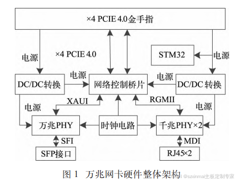
The overall hardware architecture of the 10 Gigabit network card proposed in this paper is shown in Figure 1. It mainly consists of a network control bridge chip, power module, clock circuit, 10 Gigabit PHY module, and Gigabit PHY module. Specifically, the network control bridge chip uses Intel's E810XXVDA, the 10 Gigabit PHY uses Microsemi's VSC8486, and the Gigabit PHY uses Marvell's 88E1111. This network card implements network port expansion functionality via the PCIe interface.
3 Receiver and Channel Design Requirements
From the PCIe 4.0 protocol specification [11], it is known that its receiver and channel must meet certain design requirements.
Figure 1 Overall Hardware Architecture of the 10 Gigabit Network Card
3.1 Receiver Design Requirements
PCIe high-speed serial signals are transmitted from the sender, pass through the channel, and arrive at the receiver. During this process, the signal undergoes some attenuation, leading to distortion. There are two methods for evaluating receiver signal quality. The first is the traditional time-domain transient simulation method, which suffers from slow simulation speed, low accuracy, and poor reliability. The second method is the statistical eye diagram method [12], which offers fast simulation speed, high accuracy, and high reliability. After comprehensive consideration, this paper adopts the second method to evaluate the receiver's signal quality. An eye diagram has two parameters: eye width and eye height. Only when the minimum eye width and eye height are met can the signal pass; otherwise, it fails. The PCIe 4.0 protocol specification stipulates