FPGA-based FPD-Link (LVDS 7:1) and FPD-Link II & III Implementation and Customization
This article primarily introduces the brief history of FPD-Link's development, focuses on the LVDS 7:1 technology applied in the first generation of FPD-Link, and briefly covers relevant content of the second and third generations of FPD-Link.
FPD-Link (Flat Panel Display Link) is a free, royalty-free, high-speed digital video interface standard proposed by National Semiconductor (later acquired by TI) in 1996. It was primarily applied in laptops, tablet computers, early smartphones, and LCD TVs. At its inception, it aimed to address the increasing bandwidth demands of high-resolution LCD/LED displays, which traditional TTL/CMOS parallel interfaces could not meet.
1. FPD-Link and LVDS
FPD-Link was the first large-scale application of LVDS technology proposed by NS and was recognized and accepted by the industry. Because FPD-Link is a free and open standard, it has many aliases (or mutually compatible variant standards), such as FlatLink, proposed by TI in its early years. The SPWG (Standard Panels Working Group), established at the end of the 20th century, once designated FPD-Link/FlatLink as the standard for image and video interfaces, actively promoted it in the industry, and gained recognition from some manufacturers and a certain scale of commercial use. Unfortunately, while the LVDS technology used in the first generation of FPD-Link achieved great success, FPD-Link itself could only be considered a small-scale success. Having lost out in competition with video interface standards such as DVI, HDMI, DisplayPort, and later MIPI, the SPWG was subsequently disbanded. However, this does not mean that FPD-Link completely failed. Due to its simple implementation and low cost, it held an absolute advantage in short-distance connections between circuit boards, and between display modules or camera modules and circuit boards, and achieved significant commercial adoption.
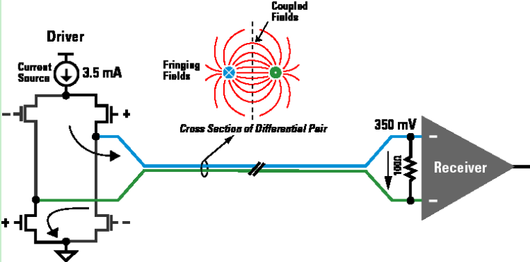
Figure 1. Basic Block Diagram of an LVDS Transceiver
FPD-Link is primarily used for RGB video interfaces. Taking RGB666 as an example, a parallel interface typically requires 22 lines, whereas FPD-Link only requires four differential pairs (one for clock, three for data). Furthermore, the application of LVDS significantly improved the EMC performance of circuit boards, enabling support for higher bandwidth and higher resolutions.

Figure 2. Schematic Diagram of an FPD-Link Interface for RGB666 Video Data Transmission (3D+C)
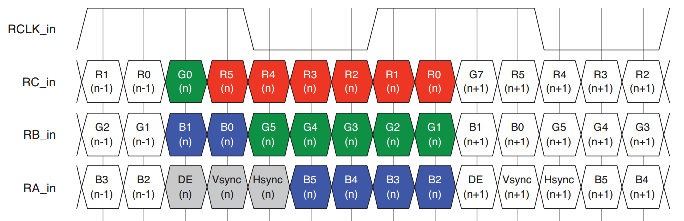
Figure 3. Schematic Diagram of RGB666 Pixel Arrangement
RCLK is the pixel clock. A total of 37=21 bits of data can be transmitted per cycle. Besides the 18 bits required for RGB666, the remaining 3 bits are used to transmit DE, Vsync, and HSync. Due to the specific phase relationship between RCLK and each data lane, it does not need to transmit synchronization words for data word alignment. Assuming RCLK is 50MHz, the interface can achieve a rate of 72*50 = 1050 Mbps.
In addition to RGB666, common forms include RGB888, RGB101010, etc., which can be implemented using 4D+C and 5D+C configurations, respectively.
Another version of FPD-Link is called OpenLDI (sometimes OpenLDI and FPD-Link refer to the same thing). Compared to basic FPD-Link, OpenLDI adds encoding functionality for DC Balance to achieve longer transmission distances. In practice, OpenLDI with added encoding functionality still has the same physical interface as FPD-Link, but requires additional encoding and decoding capabilities.
It should be noted that there are two standards for pixel mapping: one is the VESA standard, and the other is the Japanese JEIDA standard, as shown in Figure 4 and Figure 5, respectively. Since FPD-Link is an open standard, custom standards other than VESA and JEIDA can occasionally be seen.
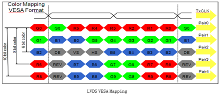
Figure 4. VESA Standard
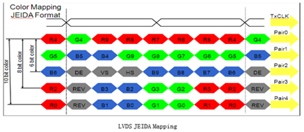
Figure 5. JEIDA Standard
2. FPD-Link II
The second generation of FPD-Link is known as FPD-Link II. To achieve higher speeds and fewer interfaces, FPD-Link II adopted a SerDes interface, replacing the LVDS 7:1 interface used in the first generation. For example, transmitting RGB888 video data with the first-generation FPD-Link required 5 LVDS differential pairs; with FPD-Link II, only one SerDes-based LVDS/CML differential pair is needed.
In addition, FPD-Link II also incorporated the DC balance encoding used in OpenLDI and adopted AC coupling on the link. These improvements allowed FPD-Link II to achieve bandwidths of up to approximately 3Gbps. Later, to enable FPD-Link II to achieve longer transmission distances and operate at speeds above 1.8Gbps in automotive and automation systems, NS replaced FPD-Link II's SerDes-LVDS interface with a SerDes-CML interface. Systems using CML (Current Mode Logic) interfaces can achieve transmission distances of up to approximately 10m.
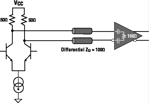
Figure 6. A Typical CML Transceiver Interface Structure
3. FPD-Link III
The third generation of FPD-Link is called FPD-Link III and was introduced in 2010. Compared to FPD-Link II, the third generation of FPD-Link added bidirectional communication capabilities and supports the transmission of low-speed signals like I2C and CAN over the link (primarily an improvement for automotive application requirements). FPD-Link III completely abandoned the SerDes-LVDS interface used in early FPD-Link II and only supports SerDes-CML interfaces. This allows it to achieve a communication distance of 10m at a rate of 3Gbps. Furthermore, FPD-Link III also supports HDCP encryption functionality and has been certified by Digital Content Protection LLC.