Signal Integrity Design and Implementation of Domestic PCIe 4.0/5.0 Switches for AI Server HBA Cards (Part 1)
0 Introduction
A Host Bus Adapter (HBA) is a circuit board or integrated circuit adapter that provides a physical connection between a computer or server and storage devices [1]. In addition to physical connection, HBAs also perform input/output processing. By using an HBA adapter card, the host's microprocessor does not need to perform data storage and retrieval operations, thereby improving server performance [2]. Peripheral Component Interconnect Express (PCIe) is a high-speed serial computer expansion bus standard. PCIe 1.0 achieves a single-lane speed of 2.5 Gb/s, while the standard transmission rate for PCIe 4.0 is as high as 16.0 Gb/s. At such high transmission rates, ensuring the signal integrity of Printed Circuit Board (PCB) routing is extremely important [3-4]. Win et al. [5] proposed a new specification technique that can accurately test the frequency domain channel bit error rate parameters of high-speed differential interfaces on PCBs, including parameters such as insertion loss, crosstalk, and reflection. Thaker et al. [6] designed a broadband differential transmission line for PCBs, used to test equalizer integrated circuits, ensuring signal integrity. Zou Jing [7] studied the signal integrity of PCB transmission lines for high-speed memory interfaces on PCBs. Wu Ling [8] used Cadence's Allegro PCB SI/PI tools to explore the theoretical basis of signal integrity related issues and proposed corresponding solutions. In reference [9], the authors of this paper designed an HBA controller chip for PCIe bus to SAS/SATA interface data transmission. They performed S-parameter simulation and eye diagram simulation on the PCIe 4.0 signals of the HBA controller chip package substrate to verify the integrity of PCIe 4.0 signals. Building on this, this paper utilizes the chip designed in reference [9] to design a PCIe 4.0 × 4 Lane/SAS 3.0/SATA 3.0 HBA card PCB. Cadence Sigrity was used to model the PCB file and perform frequency domain and time domain simulations. Through simulation experiments, the PCIe 4.0 signal integrity of the HBA card PCB was verified, completing the signal integrity research for the HBA chip from conception, from chip substrate packaging to the actual HBA card PCB.
1 HBA Card PCB Design
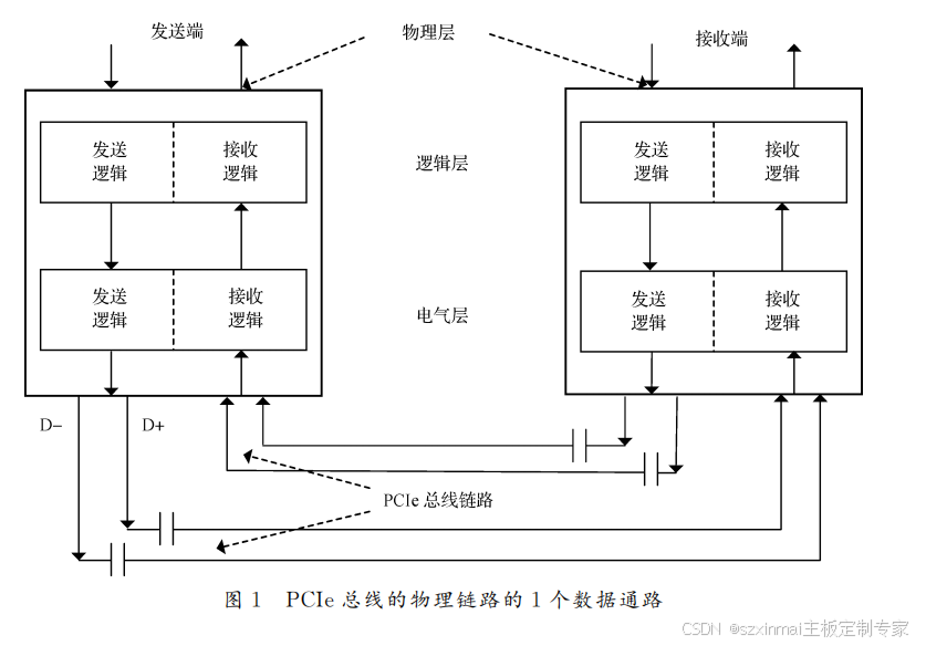
This paper uses Cadence Allegro software to design an HBA card PCB based on a PCIe 4.0 to 8-port SAS 3.0/SATA 3.0 HBA chip. The PCIe bus uses an end-to-end connection, where each end of a PCIe physical link can only connect to one device, but it can consist of multiple data paths (Lanes). The HBA card circuit studied in this paper can implement 4 Lanes. A single Lane of a PCIe bus physical link is shown in Figure 1. The PCIe bus is a high-speed differential bus, and one Lane consists of two differential pairs, each comprising four signal lines, namely Transmitter (TX) and Receiver (RX) logic.
The design of an HBA card PCB first requires consideration of factors such as signal transmission path impedance, PCB material loss factor, PCB stack-up structure, and signal traces, especially differential impedance and differential trace routing rules, which significantly impact signal integrity and power integrity [10]. The PCB dimensions are 6575 mil × 4728 mil, with a total thickness of 1.652 mm, using an 8-layer board structure. Figure 2 shows the PCB layouts for the TOP and BOTTOM layers. Table 1 presents the 8-layer stack-up information. The 8-layer structure consists of, in order, the TOP layer (primarily for RX differential signals), a solid ground plane, a high-speed signal and power plane, a power plane, a ground plane, a high-speed signal and power plane, a solid ground plane, and the BOTTOM layer (primarily for TX differential signals).
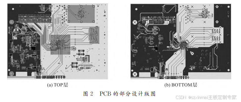
This paper uses Cadence Allegro software to design the PCB file, with some design rules as follows: The minimum trace width for outer layer differential traces is 4.2 mil, with a minimum spacing of 8.8 mil, and the differential impedance requirement is (100 ± 10) Ω; the minimum trace width for inner layer differential traces is 4.3 mil, with a minimum spacing of 8.8 mil, and the differential impedance requirement is (100 ± 10) Ω; the minimum trace width for single-ended signal traces is 5.0 mil, with a minimum spacing of 12.0 mil, and the single-ended impedance requirement is (50 ± 5) Ω. The coupling capacitor selected for PCIe 4.0 TX signals is a 0.22 μF capacitor from muRATA, model GRM033R60J224ME15.
==========================
Technical Specifications
Data Transfer Rate
12GB/s SAS 3.0 Compliant
SAS Bandwidth
Half Duplex(x8 wide bus)
9600MB/s
Port Configuration
8 ea, x1 ports (single drive)
2 ea, x4 wide ports
LED Management
SFF-8485 (SGPIO) compliant
PCI Power
13W
Host Bus
x8 lane, PCIe 3.0
PCI Data Transfer Rate
Half Duplex
x8 PCIe 3.0 8000MB/s
Environmental
Operating Temperature: 0℃-55℃
Storage: -45℃-105℃
5-90% non-condensing
Airflow: 200LFM
Integrated RAID
14 spread across 2 volumes
RAID 0 10 per volume
RAID 1 2 per volume plus hot spare
RAID 1E 10 per volume
RAID 10 10 per volume
MTBF
2,800,000 hours