STM32 ARM+FPGA+AD-based Power Quality Analyzer Design Scheme (Part 1) Software Design
Power Quality Analysis System Core Algorithms and Software Design
4.1 Software Architecture of the Power Quality Analysis System
The workflow of the power quality analysis system is as follows: After the system powers on, the ARM and FPGA perform initialization and configuration. Subsequently, a connection is established with the host computer for parameter setting. The parameters are then transmitted to the ARM. The ARM transmits control commands to the FPGA via the FSMC bus. After the FPGA executes the corresponding commands, it transmits the data back to the ARM for storage and also to the host computer for real-time display. The software design block diagram is shown in Figure 4-1.
4.1.1 System Development Process
Verilog HDL is used for RTL code writing in FPGA design, describing the functionality of the circuit. It is then converted into a gate-level netlist by synthesis tools, and a bitstream file is generated for FPGA configuration [55]. Adding constraint settings to the project file during FPGA development ensures the correctness and reliability of the design. It allows for reasonable resource allocation and avoids excessive resource utilization, thereby improving the circuit's operating speed and efficiency, optimizing circuit performance, and enhancing work efficiency. By adding simulation files to the project, designers can verify the circuit's performance and behavior under different conditions, ensuring it operates as expected.
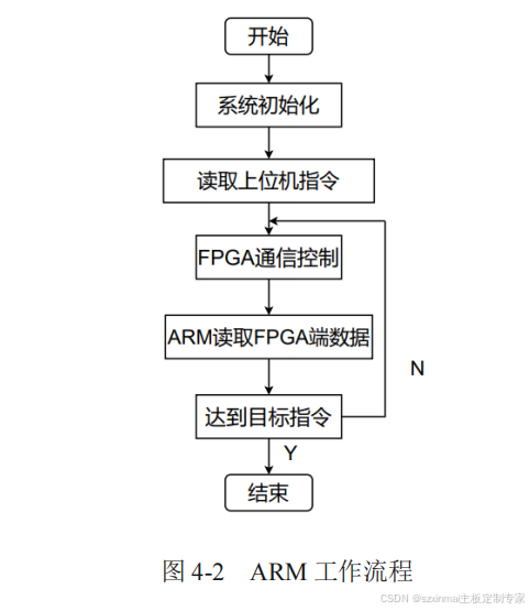
The ARM-side workflow is shown in Figure 4-2. First, initialization and configuration are performed, including system clock initialization, reading critical system configuration information, and configuring the FPGA. Subsequently, control information from the host computer is read, such as voltage detection and harmonic detection control signals. This control information is parsed and written into registers via the FSMC bus to drive the FPGA to perform corresponding tasks. After detection is complete, the power quality parameter information is read back and transmitted to the ARM for display, storage, and other operations.
4.2 FPGA Software Design
During FPGA system design, the principle of functional implementation should be followed. The system should be divided into different modules from top to bottom, with each module existing independently. Cooperative work between modules is achieved by instantiating them in the top-level module. Adopting a modular design approach can improve the system's reusability, maintainability, and testability, reducing development difficulty and risk. During design, attention should be paid to the consistency of interfaces and data formats between modules to ensure seamless cooperative operation.
4.2.1 Phase-Locked Frequency Multiplication Module
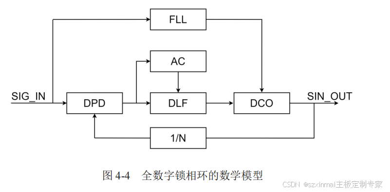
The hardware circuit performs real-time tracking of the grid frequency and processes it into a shaped square wave. The FPGA-based software design implements frequency detection, phase locking, and frequency multiplication. Compared to hardware-implemented phase-locked frequency multiplication, software-implemented PLLs offer higher flexibility and can be adjusted according to actual system requirements. This design employs an all-digital phase-locked loop (ADPLL) for synchronous sampling. Unlike traditional digital phase detectors implemented with combinational logic, which are prone to glitches when signals are unstable, leading to phase-locking failure, this design uses a digital phase detector based on sequential logic. Furthermore, a feedforward frequency detector is added to the traditional PLL to accelerate phase locking during sudden signal changes. The signal is frequency-multiplied by 500 and used as the sampling clock for the AD converter. The block diagram of the all-digital phase-locked loop is shown in Figure 4-3.

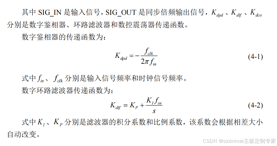
The working principle of the all-digital phase-locked loop is as follows: The digital phase detector compares the input signal and the reconstructed signal to determine the phase difference. The adaptive controller outputs different K__P and K__I parameters based on the phase difference to control the loop filter, which performs frequency division counting on the phase difference. The count value and the detected value _A_0 from the feedforward frequency detector are used as the N frequency control for the numerically controlled oscillator (NCO). This outputs a synchronously multiplied frequency signal. The mathematical model of the all-digital phase-locked loop is shown in Figure 4-4.
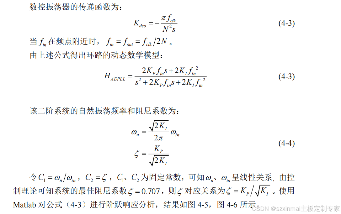
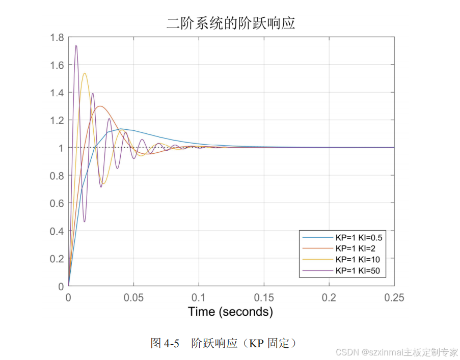
From Figures 4-5 and 4-6 above, it can be seen that when K__P is fixed, the system's response speed increases with increasing K__I values, but the stability margin decreases. When K__I is fixed, increasing K__P can accelerate the locking speed, but if K__P is too large, it will increase the system's steady-state error.
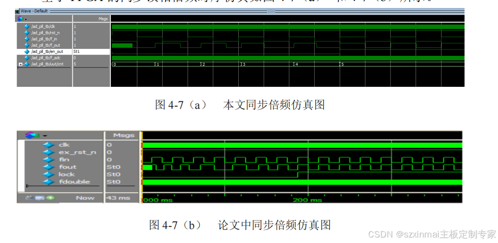
The timing simulation of the FPGA-based synchronous phase-locked frequency multiplication is shown in Figures 4-7(a) and 4-7(b).