Power Low-Voltage Protection Main Control Board Solution Based on AM62x/AM64x + FPGA
Power Low-Voltage Protection Main Control Board Solution Based on AM62x + FPGA
Specification
Description
Processor
AM6231 at up to 1.2GHz
Operating System
VXWORKS
Storage
DDR4, 8GB EMMC
Interfaces
• 1x 10/100Mbps ETH
• 1x USB2.0
• 6x KEYPAD Inputs
• 1x RS485
• 1x IRIGB
• 1x RS232
Debug Interface
JTAG / COP debug port
0 Introduction
As industrial users demand higher power supply reliability, digital protection and control devices are becoming increasingly widespread in industrial applications. Current low-voltage integrated protection devices on the market are based on a dual-CPU architecture of DSP and MCU, where the DSP is responsible for logic function calculations, and the microcontroller handles interface display and keyboard input. With the continuous advancement of IT technology, this architecture offers relatively low performance, with less fluid LCD interface operations and weaker DSP sampling data processing capabilities. For integrated protection and control functions, this performance no longer provides an advantage. Most communication between the CPU and DSP uses serial communication, lacking a data bus, which results in lower transmission reliability and hinders the expansion of modules and functions. Therefore, a high-performance acquisition platform is needed to address issues such as high-speed data transmission, large-capacity data sampling, and synchronization between protection algorithms and data sampling.
To address the above issues, this paper proposes an FPGA + DSP + CPU architecture, where the FPGA acts as a bridge for data transfer between the CPU and DSP, ensuring stable and reliable data transmission. In this architecture, the FPGA is used for analog signal acquisition and transmission in low-voltage integrated protection devices, sending the acquired data to the DSP for protection initiation and logic operations; the CAN bus is used for digital input acquisition, DC signal acquisition, and CPU management data channels.
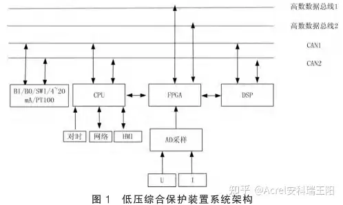
1 Overall Architecture of the Device
The overall architecture of the device is shown in Figure 1. The system employs two high-speed data buses and two CAN buses. High-speed bus communication is used for transmitting large data volumes, such as analog signal acquisition. The data bus approach facilitates the expansion of modules and the system. It utilizes LVDS differential circuits, which can suppress common-mode interference signals and enhance the device's anti-interference capability. The CAN bus is used for transmitting digital inputs/outputs, 4-20mA DC signals, PT100 temperature data, and for data transfer between the DSP and CPU. Additionally, CPU management commands and message interactions with other intelligent modules are also realized via the CAN bus. The CPU is responsible for human-machine interface functions, implementing device display, setting adjustments, event viewing, event recording, fault waveform recording, time synchronization, and network communication services. The entire system design adopts a redundant structure for high-speed data buses and CAN buses, ensuring system safety, stability, and reliable data transmission. The powerful data processing capability of the FPGA undertakes fundamental data exchange and processing tasks, providing timestamps for device messages, events, etc., while reducing the workload of the CPU and DSP. The DSP is solely used for calculating protection sampled values and processing logic functions, ensuring the independence of functional partitioning and the real-time nature of protection logic processing. The CPU is used for human-machine interface, display, communication, and clock processing tasks, and also manages other extended intelligent modules, ensuring system scalability.
2 Hardware Design of the Device
The low-voltage integrated protection device integrates line protection, motor protection, and capacitor protection functions. The device needs to acquire analog current and voltage signals, digital input signals, DC signals, and temperature sensor signals for logic operations, and perform circuit breaker tripping through output circuits.
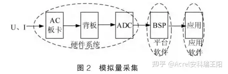
Sampling channels typically convert current and voltage signals into small voltage signals via AC conversion, which are then sent to the ADC via the backplane. After passing through a low-pass filter circuit to remove high-order harmonic interference, AD sampling converts the analog quantities into digital data, which is then sent to the FPGA for processing. The FPGA synchronizes the sampled signals obtained from the high-speed data bus and then transmits them to the DSP chip for sampling calculations and logic processing, thereby implementing the device's protection logic. Simultaneously, the FPGA sends the calculated results to the CPU for functions such as event recording, waveform storage, and LCD display. The sampling circuit needs to consider the handling of DC bias in AD chip sampling after a secondary AC circuit break. The device uses pull-down resistors to reduce the DC bias voltage, preventing excessive DC bias caused by secondary AC circuit breaks, which could lead to sampling anomaly alarms.
The analog acquisition and processing flow is shown in Figure 2.
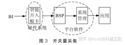
The digital input acquisition circuit, during circuit design, is compatible with DC/AC 220V, DC 110V, and DC 24V acquisition. Typically, DC 220V, DC 110V, and DC 24V acquisition is achieved through voltage divider resistors. This implementation requires either different BOMs or using jumpers to select the acquisition circuit resistors. Different BOMs require selection specifications during ordering, and the jumper method requires plugging and unplugging modules to complete jumper selection, both of which have certain drawbacks. This device's design adopts an adaptive principle, allowing for self-adaptation. It uses a setpoint adjustment method to achieve DC/AC 220V and DC 110V acquisition, facilitating engineering implementation.
The digital input acquisition and processing flow is shown in Figure 3:
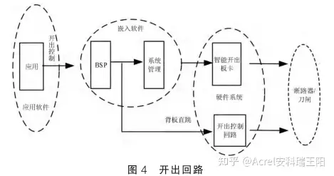
The output circuit design features two types of outputs: one is the trip signal output from logic calculations, and the other is the open/close command issued by the application backend. These two output modes are processed differently. Remote control commands from the application backend, after passing through the BSP driver and system management module, drive the output circuits of the intelligent output board, thereby controlling operating mechanisms such as disconnectors and circuit breakers. The trip signal output from the protection logic, after passing through the BSP, directly controls the output circuits of the output board via the backplane to reduce output control delay. The output circuit design is shown in Figure 4.
One-key open/close function design: Protection and control devices typically control circuit breakers using backend software or the main wiring diagram on the device interface for remote control of switching operations. In addition to supporting these functions, considering its application in low-voltage integrated protection scenarios, this device is designed with a one-key open/close button function, allowing for one-key opening and one-key closing operations via the device's front panel buttons. This function is simpler and more convenient compared to backend remote control, providing a quick way to remotely open and close switches in scenarios without a backend application.
3 Software Function Design of the Device
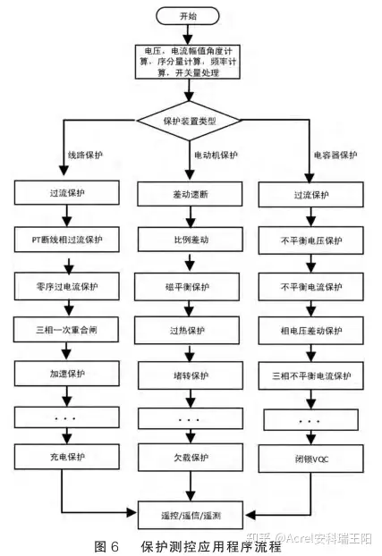
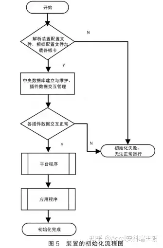
The low-voltage integrated protection device provides different protection configuration functions based on various protected objects. For different objects, the measurement and control functions serve the same purpose. Therefore, during software function design, the three sub-modules of measurement and control functions—remote control, remote signaling, and remote measurement—are treated as universal modules. For motor protection, line protection, and capacitor protection, the protection function modules differ depending on the protected object. The device allows selecting whether it is a motor protection device, a line protection device, or a capacitor protection device via protection type setpoints. According to the selected device type, corresponding protection function modules, setpoint lists, software blocking, hardware blocking, and control words will be configured. While integrating multiple protection functions, convenience for engineering implementation is considered by selecting the protection functions of the protection device through setpoint adjustments. The device initialization process is shown in Figure 5:
The platform program includes real-time modules, LCD modules, communication modules, time synchronization modules, printing modules, device debugging modules, etc. The application program is the implementation module for the device's protection and control functions. For low-voltage integrated protection devices, different application functions are available depending on the device type. The protection and control function flow is shown in Figure 6.