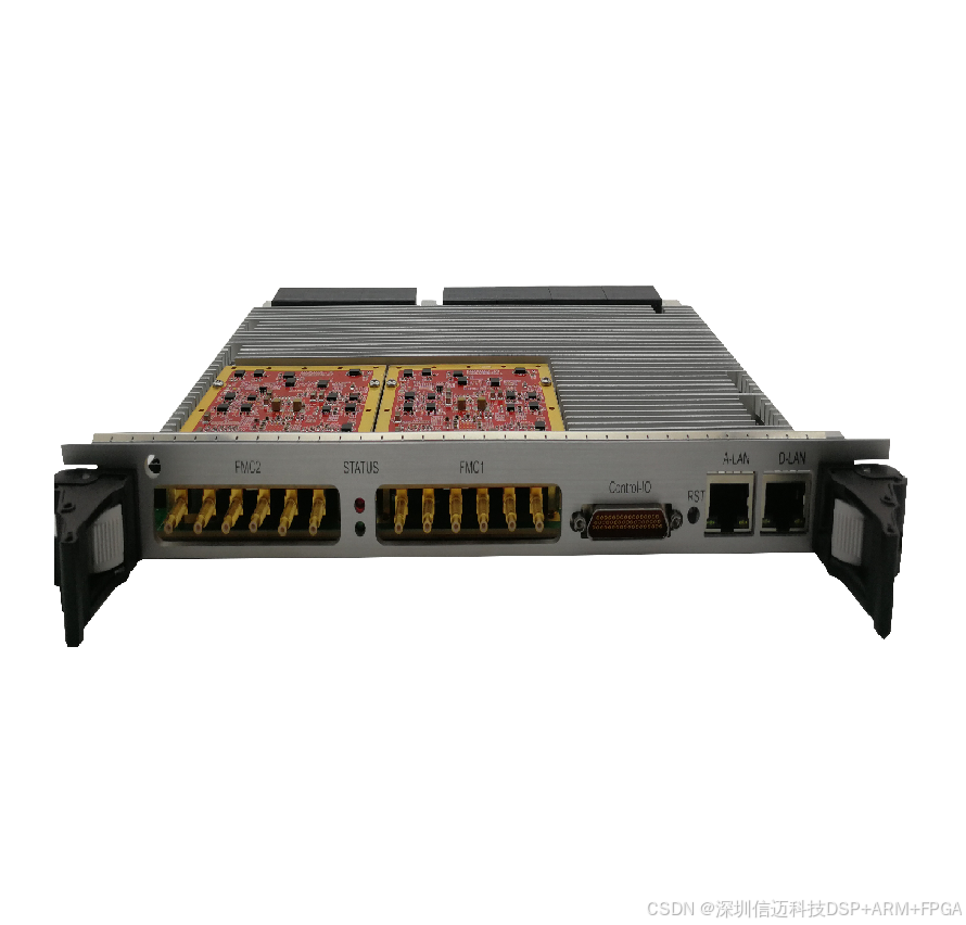
[VPX Bus] DSP+FPGA General-purpose Ultra-wideband Real-time Signal Processing Platform Based on 6U VPX Bus Architecture
- 6U VPX architecture, compliant with VITA 46 specification
- Onboard 1 TMS320C6678 multi-core DSP processing node
- Onboard 1 XCKU115 FPGA processing node
- Onboard 2 FMC+ interfaces
- 4 x4 high-speed GTH interconnects between backplanes, supporting RapidIO, PCI Express
- High-speed RapidIO interconnect between FPGA and DSP
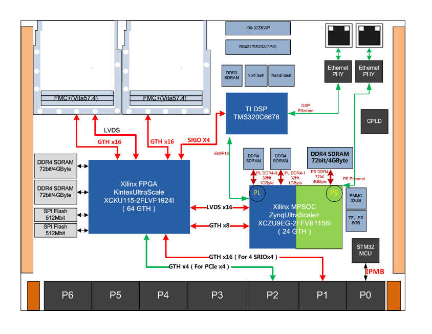
This high-speed signal processing platform is based on a 6U VPX bus architecture. It utilizes a Xilinx Kintex UltraScale series FPGA (XCKU115) as the main processor to perform complex data acquisition, playback, and real-time signal processing algorithms. A high-performance embedded processor ZU9EG with an ARM core is used as a co-processor to implement communication and management functions. The main processor XCKU115 on this platform is externally connected to two groups of 72-bit DDR4 SDRAMs to achieve ultra-large capacity data caching, with a data cache bandwidth of up to 2400MHz. The PL side of the co-processor ZU9EG on this platform supports two groups of DDR4 SDRAM. The PS side of this co-processor is a powerful ARM processor, featuring one 64-bit quad-core ARM Cortex-A53 processor, one dual-core ARM Cortex-R5 real-time processor, and one ARM Mali™-400MP graphics processor. The PS side is externally connected to 72-bit DDR4 SDRAM, supporting ECC verification. To accommodate complex floating-point signal processing algorithms, this platform also supports one TI Keystone series multi-core DSP TMS320C6678, which can perform various data processing tasks with high real-time requirements. This board features excellent anti-vibration design, heat dissipation performance, and unique environmental protection design, making it suitable for aerospace, aviation, marine, and other application scenarios.
Functional Block Diagram
Technical Specifications
- Standard 6U VPX specification, compliant with VITA 46;
- 2 multi-core DSP processing nodes, 1 Virtex-7 FPGA processing node;
- Processing Performance:
- DSP Fixed-point operations: 40 GMAC/Core * 16 = 640 GMAC;
- DSP Floating-point operations: 20 GFLOPs/Core * 16 = 320 GFLOPs;
- Storage Performance:
- DSP Processing Node: 4 GByte DDR3-1333 SDRAM;
- DSP Processing Node: 4 GByte Nand Flash;
- FPGA Processing Node: 2 groups of 2 GByte DDR3-1600 SDRAM;
- Interconnect Performance:
- DSP to DSP: HyperLink x4 @ 5 Gbps/lane;
- DSP to FPGA: SRIO x4 @ 5 Gbps/lane;
- FPGA to FPGA: 2 x GTH x8 @ 10 Gbps/lane;
- FPGA to Host Controller: PCI Express x4 @ 8 Gbps/lane;
- FPGA to FMC Interface: 2 x GTH x4 @ 10 Gbps/lane;
- Physical and Electrical Characteristics
- Board Dimensions: 100 x 233 mm
- Board Power Supply: 5A max @ +12V (±5%)
- Cooling Method: Conduction cooling (metal)
- Environmental Characteristics
- Operating Temperature: -40°C ~ +85°C, Storage Temperature: -55°C ~ +125°C;
- Operating Humidity: 5% ~ 95%, non-condensing
Application Areas
- Software Defined Radio (SDR);
- Radar and Baseband Signal Processing;