SerDes Design Solution for LS1046A & LS1028A + FPGA Platforms
In this issue, we will dedicate an article to the SerDes resource allocation for this series of platforms.
The LS series products boast abundant resources, among which the SerDes protocol is often the most perplexing. Baidu Baike explains it as follows: SERDES is an abbreviation for SERializer/DESerializer.
It is a mainstream time-division multiplexing (TDM), point-to-point (P2P) serial communication technology. Specifically, at the transmitting end, multiple low-speed parallel signals are converted into high-speed serial signals, which then travel through a transmission medium (optical fiber or copper cable), and finally, at the receiving end, the high-speed serial signals are converted back into low-speed parallel signals. This point-to-point serial communication technology fully utilizes the channel capacity of the transmission medium, reduces the number of required transmission channels and device pins, enhances signal transmission speed, and thus significantly lowers communication costs.
Let's start by explaining the most complex LS1046A.
PART.1 LS1046A
As shown in the block diagram below, there are 2 SerDes modules, each with 2 PLLs and 4 lanes, totaling 4 PLLs and 8 lanes, supporting Ethernet, PCIe, and SATA functionalities.
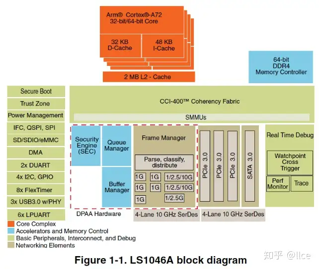
Chapter 31 "SerDes Module" in the "LS1046 ARM" document describes this part in detail, so I also recommend users review this section before finalizing their design. We list all SerDes functionalities of the LS1046A:
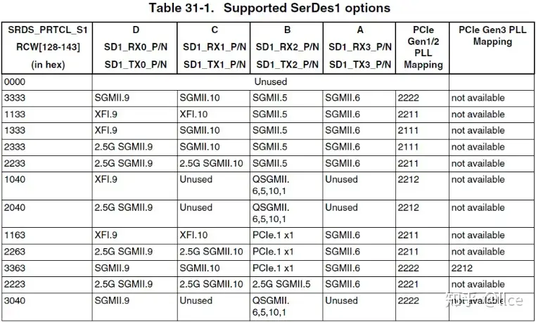
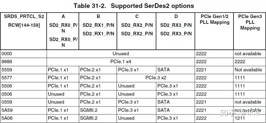
The first column represents the RCW bits, and the design scheme can only be selected from these options (thus, configuring all 8 lanes as Ethernet ports is not possible); the subsequent columns A, B, C, D represent the hardware signal names and interface functionalities; the last two columns are for PLL configuration. Pay attention to the term "Mapping," which indicates whether you need to configure PLL1 or PLL2. For example: "2222" means all four lanes A, B, C, D use PLL2; "2211" means lanes A, B use PLL2, and lanes C, D use PLL1. "not available" means this scheme does not support PCIe Gen3 speed.
XFI, SGMII, and QSGMII are all network interfaces. SGMII.n indicates 1G speed, where 'n' refers to the MAC; QSGMII includes 4 MACs, each operating at 1G speed; XFI operates at 10G speed. When configuring Ethernet ports, it's crucial to ensure MACs do not conflict.
For PCIe.n, 'n' represents the PCIe identifier. For easier understanding, 'n' can be considered the Root Complex (RC) identifier. Configuration conflicts are not allowed. For example, configuring SerDes1 as '1163' and SerDes2 as '5559' is incorrect because PCIe.1 is duplicated. PCIe.nx4 means 4 lanes are combined into a single PCIe RC, which can only connect to one EP (endpoint device), and the speed will be quadrupled (x4).
SATA needs no further explanation; simply select it from the available options.
After selecting the function for each lane, you also need to choose the SerDes reference clock. The clocks required for each function are shown below:
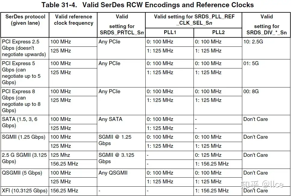
These are PLL1 and PLL2 that we need to configure; both hardware and software configurations must be done correctly. The reference clock source has already been implemented on our core board, so users do not need to perform additional hardware work for this part. Specifically, it is implemented as follows:
SerDes2 only supports PCIe, SATA, and SGMII (1.25G) functionalities. All three can reference a 100MHz clock. Our core board's hardware is fixed at 100MHz, so only software selection of the PLL is required.
SerDes1 supports SGMII (1.25G), SGMII (3.125G), QSGMII, XFI, and PCIe functionalities. As shown in Table 31-4, PLL1 for these functions can all be set to 100MHz. Therefore, our core board's hardware is fixed at 100MHz. PLL2 can reference 100MHz and 156.25MHz to enable all functionalities. We route an SD1_REFCLK_SEL pin from the core board to select between 100MHz and 156MHz, and then software configures the corresponding PLL.
Therefore, for our core board, SerDes2's PLL1 and PLL2 can only be set to 100MHz; SerDes1's PLL1 is fixed at 100MHz, and SerDes1's PLL2 can be selected between 100MHz and 156MHz.
The corresponding SerDes module can be disabled by turning off its PLL.
If this explanation is still unclear, let's take an example. Suppose a project requires one 10 Gigabit Ethernet port