FPGA+DSP Architecture-based Intermediate Frequency Signal Acquisition, Processing, and Remote Optical Fiber Transmission System for Radar Applications
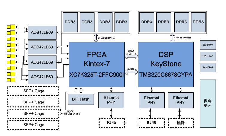
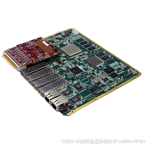
This is a high-performance radar signal real-time acquisition and processing platform based on optical fiber transmission. The platform integrates an I/O unit, a signal processing unit, and a remote transmission unit, enabling real-time acquisition, real-time processing, high-speed transmission, and high-speed storage of radar signals. The system platform consists of one signal processing platform card and one 4-channel optical fiber acquisition card, as shown in Figure 1. The signal processing platform is equipped with one 8-channel, 250 MSPS sampling rate, 16-bit AD acquisition FMC daughter card. The system's operating principle is as follows: 8 channels of analog AD signals (from the antenna array) enter four high-speed ADCs via SSMC interfaces. The FPGA drives these four high-speed ADCs and completes real-time synchronous data acquisition of analog intermediate frequency signals. The FPGA features large-capacity on-board caching and performs complex algorithm processing, precisely measuring the phase of multiple antenna arrays entirely from a time-domain perspective. The signal processing board also features one TI multi-core DSP processor C6678 for fast spectrum analysis. Real-time data sharing between the FPGA and DSP is achieved via a high-speed interface, enabling powerful signal processing capabilities from both time-domain and frequency-domain perspectives. The platform uses single-mode or multi-mode optical fiber for remote transmission, and high-speed serial communication ensures that acquired data is updated in real-time on the server. This system achieves real-time acquisition, real-time processing, remote transmission, and high-speed storage of radar signals. It widely uses high-speed serial buses such as SRIO, PCIe, and Ethernet for data transmission, offering advantages such as high performance, high availability, and high reliability.
- Supports 8 channels of 250 MSPS sampling rate, 16-bit analog signal input
- Supports 4 SFP+ optical fiber channels, with up to 10Gbps/lane
- On-board 1 XC7K325T FPGA processor
- On-board 1 TMS320C6678 multi-core processor
- Supports 2 Gigabit Ethernet ports
- Supports multi-system cascading and synchronous acquisition
Functional Block Diagram
Technical Specifications
- System Composition:
- One 8-channel, 250 MSPS sampling rate, 16-bit resolution AD acquisition FMC daughter card (Model: FMC128);
- One FPGA + DSP signal processing board (Model: TES600);
- One 4-channel optical fiber acquisition card (Model: PCIE730);
- System Interconnection:
- AD daughter card and signal processing board: FMC high-speed connector LVDS interconnection;
- Signal processing board and optical fiber acquisition card: Interconnected via single-mode or multi-mode optical fiber;
- Optical fiber acquisition card and server: Interconnected via PCIe bus;
- Acquisition Performance:
- Maximum support for 8-channel, 250 MSPS sampling rate, 16-bit resolution real-time acquisition;
- Input voltage range: 1Vpp (4dBm) ~ 2Vpp (10dBm), programmable input voltage range;
- Analog input bandwidth: 500MHz (typical);
- SFDR@170MHz: 87dBc;
- SNR@170MHz: 73.2dBFS;
- ENOB@170MHz: 11.85bits;
- 8-channel AD synchronous acquisition;
- Processing Performance (Signal Processing Board):
- DSP fixed-point operations: 40 GMAC/Core * 8 = 320 GMAC;
- DSP floating-point operations: 20 GFLOPs/Core * 8 = 160 GFLOPs;
- Transmission Performance:
- Supports Serial RapidIO, Aurora, and other transmission protocols;
- Serial RapidIO supports 6.25Gbps line rate, Aurora supports 10Gbps line rate;
- Supports single-mode or multi-mode optical fiber, maximum transmission distance 80KM;
- Storage Performance:
- Storage bandwidth: 64-bit, DDR3 SDRAM, 500MHz operating clock;
- Storage capacity: Maximum support for 4GByte DDR3 SDRAM;
- Other Interface Performance:
- One high-precision clock unit, supporting 1 external clock input, 2 synchronous clock outputs;
- 2 RS485 interfaces, 4 LVTTL inputs, 4 LVTTL outputs;
- On-board 1 FRAM memory, 1 BPI Flash;
- Physical and Electrical Characteristics
- Board dimensions: 100 x 160mm
- Board power supply: 1.5A max@+12V (±5%)
- Cooling method: Metal conduction cooling
- Environmental Characteristics
- Operating temperature: -40°C ~ +85°C;
- Storage temperature: -55°C ~ +125°C;
- Operating humidity: 5%~95%, non-condensing
Software Support
- Optional integrated Board Support Package (BSP);
- FPGA low-level interface drivers;
- DSP low-level interface drivers;
- Board-level interconnection interface drivers;
- Customizable algorithms and system integration can be provided according to customer requirements:
Application Areas
- Software-defined radio;
- Radar and baseband signal processing;