4-Channel Cameralink Base Image Emulator Based on FPGA (K7) and PXIe Bus Architecture
Software Support
- Optional integrated board-level software development kit (BSP);
- FPGA low-level interface drivers;
- Board-level interconnect interface drivers;
- Customized algorithms and system integration can be provided according to customer requirements:
Application Areas
-
Software-defined radio (SDR);
-
Radar and baseband signal processing;
-
High-speed image and graphics processing;
-
Standard 3U PXIe form factor
-
Supports 4-channel Cameralink Base image output
-
Onboard 1 XC7K325T FPGA processor
-
Supports x8 PCIe host interface, system bandwidth 4 GByte/s
-
Onboard HJ30J connector, supports 4 Cameralink interfaces
-
Supports RS232/RS422/RS485 interfaces
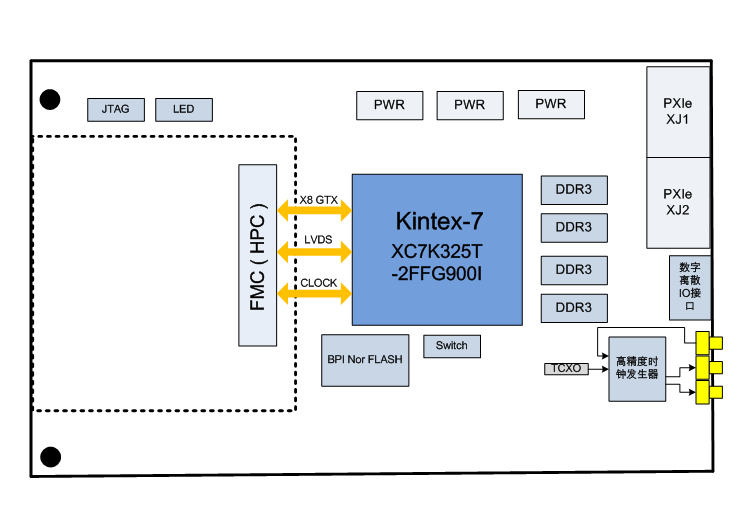
A 4-channel Cameralink Base image emulator based on the PXI Express bus architecture. This board features one FMC (HPC) interface and one x8 PCIe host interface. The board utilizes a high-performance Xilinx Kintex-7 series FPGA as its real-time processor to achieve data acquisition and processing from the FMC interface, as well as conversion for the PCI Express bus interface. It includes one independent 64-bit DDR3 SDRAM large-capacity cache. By integrating different FMC daughter cards, this board can quickly establish a verification platform based on the PXI Express instrument bus. This board is a standard 3U PXI Express size, suitable for standard Eurocard PXIe chassis, and can be widely applied in scenarios such as radar and IF signal acquisition, and video image acquisition.
Technical Specifications
- Onboard FPGA real-time processor: XC7K325T-2FFG900I;
- Host Interface Specifications:
- Compliant with PXIe standard, supports PCI Express 2.0 specification;
- Supports PCIe Gen2 x8@5Gbps/lane;
- PCIe bidirectional DMA transfer bandwidth: 3.2 GByte/s;
- FMC Interface Specifications:
- Standard FMC (HPC) interface, compliant with VITA57.1 specification;
- Supports x8 GTX@10Gbps/lane high-speed serial bus;
- Supports 80 pairs of LVDS signals;
- Supports IIC bus interface;
- +3.3V/+12V/+VADJ power supply, power supply capability ≥15W;
- Independent VIO_B_M2C power supply (can be provided by daughter card)
- Dynamic Storage Performance:
- Storage bandwidth: 64-bit, DDR3 SDRAM, 500MHz operating clock;
- Storage capacity: Maximum support for 4 GByte DDR3 SDRAM;
- Other Interfaces:
- 1 high-precision clock unit, supports 1 external clock input, 2 synchronous clock outputs;
- 2 RS485 interfaces, 4 LVTTL inputs, 4 LVTTL outputs;
- Onboard 1 FRAM memory, 1 BPI Flash;
- Physical and Electrical Characteristics
- Board dimensions: 100 x 160mm
- Board power supply: 1.5A max@+12V (±5%)
- Cooling method: Metal conduction cooling
- Environmental Characteristics
- Operating temperature: -40°C to +85°C;
- Storage temperature: -55°C to +125°C;
- Operating humidity: 5%~95%, non-condensing
Functional Block Diagram