X86/ARM Industrial PC + K7 FPGA AI Data Processing Platform, Applicable to Radar and IF Signal Acquisition, Video Image Acquisition and Transmission, and Other Application Scenarios.
Product Overview
This high-performance data pre-processing FMC carrier board is based on a PCI Express bus architecture. The board features one FMC (HPC) interface and one x8 PCIe host interface. It utilizes a Xilinx high-performance Kintex-7 series FPGA as the real-time processor to achieve data acquisition and processing from the FMC interface, as well as conversion for the PCI Express bus interface. An independent 64-bit DDR3 SDRAM large-capacity cache is onboard. By integrating different FMC daughter cards, this board can quickly establish a PCI Express bus-based verification platform. As a standard full-height, half-length PCIe card, it is suitable for use in PCIe industrial PCs and applicable to scenarios such as radar and IF signal acquisition, and video image acquisition and transmission.
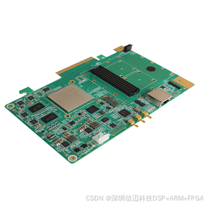
- Standard PCIe full-height, half-length card
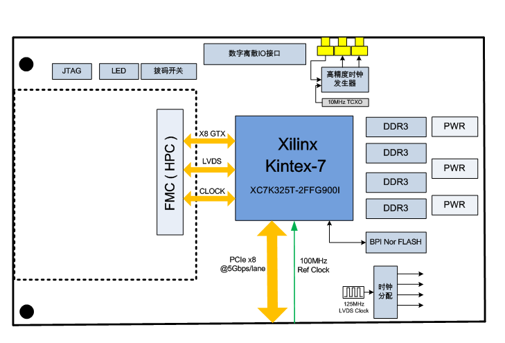
- 1 FMC (HPC) interface, compliant with VITA57 specification
- Onboard 1 XC7K325T FPGA processor
- Supports x8 PCIe host interface, system bandwidth 4 GByte/s
- Onboard high-precision clock generator
- Supports RS232/RS422/RS485 interfaces
Functional Block Diagram
Technical Specifications
- Onboard FPGA Real-time Processor: XC7K325T-2FFG900I;
- Host Interface Specifications:
- Compliant with PCIe standard, supports PCI Express 2.0 specification;
- Supports PCIe Gen2 x8@5Gbps/lane;
- PCIe Bidirectional DMA Transfer Bandwidth: 3.2 GByte/s;
- FMC Interface Specifications:
- Standard FMC (HPC) interface, compliant with VITA57.1 specification;
- Supports x8 GTX@10Gbps/lane high-speed serial bus;
- Supports 80 pairs of LVDS signals;
- Supports IIC bus interface;
- +3.3V/+12V/+VADJ power supply, power consumption ≥15W;
- Independent VIO_B_M2C power supply (can be provided by daughter card)
- Dynamic Storage Performance:
- Storage Bandwidth: 64-bit, DDR3 SDRAM, 500MHz operating clock;
- Storage Capacity: Maximum support for 4 GByte DDR3 SDRAM;
- Other Interface Performance:
- 1 high-precision clock unit, supports 1 external clock input, 2 synchronous clock outputs;
- 2 RS485 interfaces, 4 LVTTL inputs, 4 LVTTL outputs;
- Onboard 1 FRAM memory, 1 BPI Flash;
- Physical and Electrical Characteristics
- Board Dimensions: 100 x 160mm
- Board Power Supply: 1.5A max@+12V (±5%)
- Cooling Method: Metal conduction cooling
- Environmental Characteristics
- Operating Temperature: -40°~﹢85°C;
- Storage Temperature: -55°~﹢125°C;
- Operating Humidity: 5%~95%, non-condensing
Software Support
- Optional integrated Board Support Package (BSP);
- FPGA low-level interface drivers;
- Board-level interconnect interface drivers;
- Customizable algorithms and system integration can be provided based on customer requirements:
Application Areas
- Software-Defined Radio (SDR);
- Radar and Baseband Signal Processing;
- High-Speed Image and Graphics Processing;