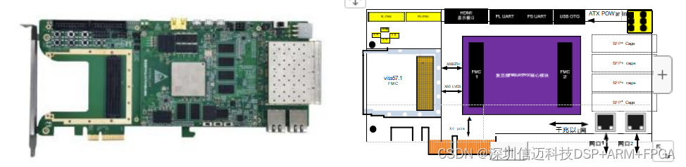
Fudan Micro FMQL45T900 ARM+FPGA+AD Fully Localized Solution, Compatible with XILINX's XC7Z045-2FFG900I (i.e., ZYNQ7045)
A fully localized ARM core board based on Shanghai Fudan Microelectronics FMQL45T900. This core board integrates the minimum system of Fudan Micro's FMQL45T900 (compatible with XILINX's XC7Z045-2FFG900I) onto an 87*117mm core board. It can serve as a core module for functional expansion, enabling rapid construction of a signal platform, facilitating product development for users. The core board features DDR3 SDRAM, EMMC, SPI FLASH, Ethernet PHY chips, and more. PL-side I/O expansion is achieved through two board-to-board FMC connectors.
The FMQL45T900 is a fully programmable fusion chip developed by Fudan Microelectronics. It integrates a Processing System (PS) based on a feature-rich quad-core processor and Programmable Logic (PL) on a single chip, utilizing the most advanced 28nm process technology. Coupled with corresponding development software, it enables an integrated hardware and software platform, facilitating user development, shortening development cycles, and saving production costs.
Technical Specifications
- Onboard Fudan Micro FPGA Programmable Fusion Chip:
-
FPGA Model: Fudan Micro FMQL45T900;
-
System-on-Chip (PS): Quad-core processor, max frequency 1GHz;
-
Logic Resources (PL): 350K logic cells, 19.2Mb Block RAM;
-
Logic Resources (PL): 16 GTX transceivers, 900 DSP slices;
- Module Main Storage and Interface Resources:
-
PS-side Memory: 1 group DDR3 SDRAM, 32-bit, 1GByte capacity;
-
PS-side Other Storage Resources: 1 EMMC (8GByte), 1 SPI Flash (256Mbit capacity);
-
PS-side Network: 1-channel 1000BASE-T adaptive Gigabit Ethernet;
-
PS-side Clock: 1x 33.333MHz crystal oscillator, system clock;
-
PL-side Memory: 1 group DDR3 SDRAM, 64-bit, 2GByte capacity;
-
PL-side Clock: 1x 50MHz crystal oscillator, logic clock;
-
Board supports watchdog reset;
- Interconnect Interfaces:
-
Interface Connectors: 2 FMC connectors;
-
FMC1: 8 GTX transceivers, 17 LVDS pairs, 28 PS MIO;
-
FMC2: 8 GTX transceivers, 80 LVDS pairs;
- Physical and Electrical Characteristics
-
Board Dimensions: 87 x 117mm;
-
Board Power Supply: 2A max@+12V (±5%);
-
Cooling Method: Natural air cooling;
- Environmental Characteristics
-
Operating Temperature: -40°~﹢85°C;
-
Storage Temperature: -55°~﹢125°C;
-
Operating Humidity: 5%~95%, non-condensing;
Software Support
- Integrated Board Support Package (BSP):
-
Supports PS-side development technical support;
-
Supports PL-side extended applications and support;
- Customizable algorithms and system integration can be provided based on customer requirements:
Application Areas
l Industrial control signal processing;
l Intelligent signal processing;
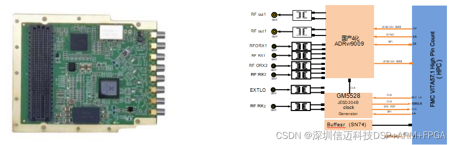
The FMC9009 is an RF submodule based on the VITA57.1 standard, implementing 2 transmit and 2 receive channels. This board is based on the localized ADRV9009 RF transceiver, covering the 50MHz~6GHz frequency band, and integrates a dual-channel transmit and receive link. The maximum real-time transmit bandwidth can reach 450MHz, and the maximum receive bandwidth can reach 200MHz, making it a highly integrated general-purpose software-defined radio platform.
The board supports external reference clock and external local oscillator input, and can be flexibly configured via software.
This board is primarily used for multi-channel RF transceivers in high-performance and low-power scenarios required by 3G/4G/5G macro base stations, micro base stations, and similar applications.
