Avionics Network (ARINC818 Bus) / CVBS / HDMI / PCIe Video Card Solutions
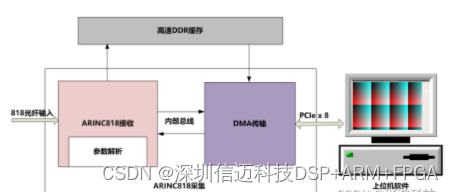
- ARINC818 Acquisition Card The ARINC818 acquisition card is a high-performance PCIe video fiber optic acquisition and test equipment designed for the Avionics Digital Video Bus (ADVB) protocol. The ARINC818 protocol is primarily used for real-time high-definition image transmission between airborne equipment and has been successfully applied in various civil and military aircraft models, making it one of the future development directions for airborne video transmission buses.
The ARINC818 acquisition card utilizes a highly integrated FPGA chip to implement the ARINC818 protocol and achieves real-time high-definition image software acquisition through a high-speed 8xPCIe interface.
Functional Block Diagram:
Application Areas
Avionics bus communication, marine data transmission bus, aerospace equipment bus communication, ground bus communication and test systems
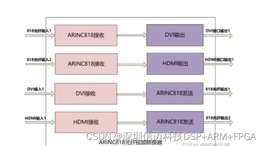
- ARINC818 Fiber Optic Video Converter The ARINC818 fiber optic video converter is a high-performance video fiber optic conversion and test equipment designed for the Avionics Digital Video Bus (ADVB) protocol. It uses a highly integrated FPGA chip to implement the ARINC818 protocol and provides high-speed real-time conversion functionality with Digital Visual Interface (DVI) and HDMI.
Functional Block Diagram:
Application Areas:
Testing of avionics ARINC818 bus communication products, testing of marine data transmission bus communication products, testing of aerospace equipment bus communication products, and various ground bus communication verification and test systems.
- H.264 IP CORE The H.264 video codec (encoder & decoder) is implemented using Verilog Hardware Description Language. This IP design can be integrated into a Field-Programmable Gate Array (FPGA) platform after compilation with FPGA EDA tools. Alternatively, it can be synthesized using Synopsys Design Compiler and used as an IP core for ASIC chips. The video encoder's output bitstream fully complies with the H.264 video coding standard; the decoder can decode bitstreams encoded by H264_Lite itself.
The design has been structurally optimized for hardware area, encoding frame rate, and synthesis frequency. This design features special timing optimizations for FPGA implementation. It can be synthesized to 125MHz on a Xilinx Zynq7020. A single core can achieve 1080P@30fps FPGA application scenarios, while a dual core can achieve 1080P@60fps application scenarios.
Product Features:
High encoding/decoding frame rate: The theoretical encoding/decoding clock frequency for 1080P30 is 110MHz. Small hardware footprint: On Zynq7020, it only occupies 55% of logic resources. Low latency: Encoder latency is within 20ms. Error control: Special handling has been implemented for scenarios where data integrity is not guaranteed, such as wireless transmission (e.g., Wi-Fi, microwave) and drone applications. Bitrate control: QP can be adjusted in MB units for smoother bitrate. Ultra-long GOP support: Up to 256 frames can pass before encoding an I-frame, reducing bitstream bandwidth peaks while maintaining excellent fault tolerance. Encoder and decoder are integrated, sharing hardware logic for a smaller area.
Customization supported. In-house R&D and manufacturing.