Data Acquisition Cards: Reliable Products Require Robust EMC Countermeasures
Brief Introduction to EMC
EMC (Electromagnetic Compatibility) is defined as "the ability of equipment and systems to function satisfactorily in their electromagnetic environment without introducing intolerable electromagnetic disturbances to anything in that environment." 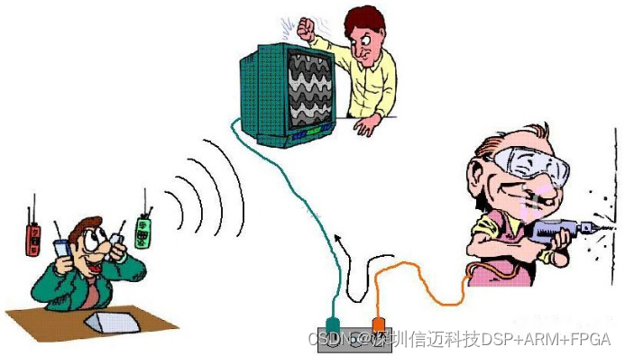
EMC encompasses two aspects: first, the device's ability to resist interference and operate normally (i.e., EMS); second, the requirement that electromagnetic emissions from the device do not affect the normal operation of other equipment (i.e., EMI).
A good design must ensure: not being disturbed by others, and not disturbing others.
EMC Design
1. Scope of EMC Design:
EMC design includes: signal design, circuit design, shielding, grounding, filtering, and proper layout. Among these, the aspects most closely related to mechanical structure are: shielding, grounding, and proper layout (Note: This does not mean other measures are entirely unrelated to structural design; structural design must also support the implementation of other measures, such as rational layout).
2. Fundamental Objectives of EMC Design:
- Internal circuits of the product do not interfere with each other and achieve intended functionality.
- The intensity of electromagnetic emissions from the product remains below specified limits.
- The product has a certain level of immunity to external electromagnetic interference.
3. Cost of EMC Design Across Product Development Phases:
In the early stages of product design, there are more options for resolving EMC issues at lower cost. However, implementing technical measures to solve EMC problems in later production stages will be constrained by various factors. Moreover, applying the same technical solutions during later stages significantly increases product cost and extends development time.
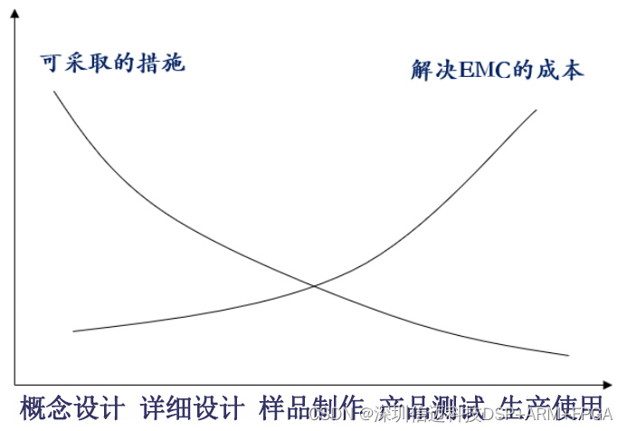
Cost of EMC Design at Various Stages of Product Development
Therefore, the cost of addressing EMC issues increases as product development progresses. Hence, EMC design should be initiated as early as possible—never wait until EMC testing reveals problems before hastily searching for root causes and solutions.
4. Traditional EMC Countermeasures:
When actual product testing occurs and EMC issues arise, engineers begin identifying the problems using tools such as spectrum analyzers and near-field probes. At this point, the only available methods are shielding and filtering. The limitations of traditional EMC countermeasures include:
- Cannot address internal EMI issues (e.g., between boards or within board signals) using shielding/filtering.
- Shielding and filtering often require design modifications, increasing product cost and development cycle time.
- Filtering is ineffective when signal and interference frequencies coincide; at high frequencies, traces, shields, and enclosures can act as antennas.
- High-frequency signals couple onto cables, which then radiate emissions.
- In the final stage of product development, shielding and filtering are the only remaining options for solving EMC issues—but can shielding alone resolve all EMC problems?
- Risks of shielding strategies: deformation or damage to enclosures and shielding materials can lead to electromagnetic leakage.
- The outcome of such countermeasures: may help pass EMC tests, but can worsen internal interference, affect system stability, and increase immunity requirements.
5. New Concept in EMC Countermeasures: 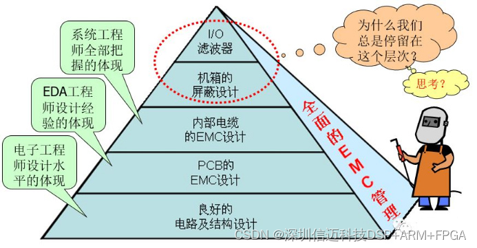
▲ Comprehensive EMC Management
The new approach to EMC countermeasures emphasizes comprehensive EMC management and early-stage EMC design:
- EMC is a systems engineering effort: early consideration leads to lower cost, more available techniques, and higher efficiency; requires collaboration across the product development team, including mechanical design.
- Make full use of existing EMC design standards and guidelines (expert experience), but critically evaluate: Can all designs strictly follow the rules? Are all theories valid in every scenario?
- Leverage simulation tools to identify and resolve issues early. PCB design simulation: HyperLynx. Electronic circuit simulation: Pspice, Serenade.
- Balance accuracy and speed; solve real-world problems with practical methods. Use measurement techniques and general instruments for comparative testing. Introduce electromagnetic field scanning for EMC pre-compliance testing.
6. EMC Design Process: 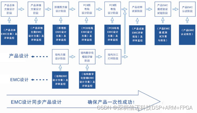
7. Experience in EMC Mechanical Design:
- Get involved in mechanical design early in the project. Hardware engineers should lead the hardware system’s mechanical design rather than passively accepting an existing mechanical structure and then struggling to meet performance and EMC requirements within its constraints. They should play a leading role in shaping the mechanical design.
- Generate 3D models early and organize cross-functional team reviews to evaluate trade-offs. From an EMC perspective, use the 3D model to identify and resolve potential issues. This interactive process should be repeated multiple times until a satisfactory result is achieved.
- Use of shielding structures: determine which boards require shielding and which do not; implement preventive EMC measures for unshielded boards; consider the PCB itself as a potential EMC shield.
- Cable management: include internal module interconnects (exposed outside the shielded enclosure) and external interface cables; ensure filtering provisions are reserved on motherboards, connection boards, or output boards.
8. EMC PCB Design
(1) PCB Design a. Layout: Group similar circuits together, follow minimum path principle, avoid placing high-speed circuits near small panels, place power modules close to the board’s power entry point; b. Layering: High-speed routing layers must be adjacent to a ground plane; power and ground layers should be adjacent; place a ground layer beneath component layers; preferably assign both outer layers as ground; inner layers should be inset by 20H relative to outer layers; c. Routing: Follow 3W rule; keep differential pairs equal in length and routed closely; high-speed or sensitive traces must not cross split planes; d. Grounding: Separate grounding for similar circuits, connected at a single point on the board; e. Filtering: Design board-level filtering circuits for power modules and functional circuits; f. Interface Circuit Design: Design filtering circuits for interfaces to achieve effective internal-external isolation.
(2) Basic Principles of Layout: a. Refer to functional block diagrams, follow signal flow, and divide layout by functional modules; b. Separate digital and analog circuits, high-speed and low-speed circuits, and noise sources from sensitive circuits; c. Avoid placing sensitive or strongly radiating components on the solder side of the board; d. Minimize loop area for sensitive signals and high-radiation signals; e. Keep strong radiation or sensitive components such as crystals, oscillators, relays, and switch-mode power supplies away from board handles, external connectors, and sensitive devices—recommended distance ≥1000 mil; f. Sensitive components: keep ≥1000 mil away from strong radiation sources; g. Isolation devices, A/D converters: separate inputs and outputs with no coupling paths (e.g., adjacent reference planes); preferably span corresponding split areas.
(3) Special Component Placement: a. Power section (placed near power entry); b. Clock section (kept away from apertures, close to load, routed on inner layers); c. Inductors (kept away from EMI sources); d. Bus driver section (routed on inner layers, away from apertures, close to destination); e. Filtering components (input and output separated, placed close to source, with short leads);
(4) Bulk Capacitor Placement: a. At all branch power interface circuits; b. Near high-power components; c. In areas with large current fluctuations, such as input/output of power modules, fans, relays; d. At PCB power interface circuits;
(5) Decoupling Capacitor Placement: a. Close to power pins; b. Appropriate location and quantity;
(6) Basic Principles for Interface Circuit Layout:
Place filtering, protection, and isolation components near interface connectors—protection first, then filtering;
Ensure complete isolation between primary and secondary sides for interface transformers and optocouplers;
No signal crossovers between transformers and connectors;
Minimize component placement on the BOTTOM layer beneath transformers;
Place interface ICs (Ethernet, E1/T1, serial ports, etc.) as close as possible to transformers or connectors;
(7) Routing
Keep traces short; maintain wide spacing between different types of traces (except signal and return paths, differential pairs, and shield grounds); minimize vias; avoid loops; reduce loop area; eliminate stubs;
For timing-critical signals, ensure trace lengths meet requirements;
Avoid right angles; prioritize rounded corners for critical signals;
Route adjacent layer signals perpendicularly, or keep parallel routing of critical signals on adjacent layers ≤1000 mil;
Ensure trace width consistency or meet impedance requirements;
(8) Product Safety and EMC Certification Bodies by Country
- Europe: CE
- United States: FCC & UL, NEBS
- Japan: VCCI
- Australia: C-Tick (Note: Original text says "CE", likely incorrect)
- China: CCC
- Taiwan: BSMI (Note: Original text says "CE", likely incorrect)
- CISPR: International Special Committee on Radio Interference
- TC77: Technical Committee on Electromagnetic Compatibility within Electrical Equipment (including power systems)
- TC65: Industrial Process Measurement and Control
(9) Product Certification Process
- Certification application
- Submission of certification materials (standards, user manuals, etc.)
- Product testing
- Completion of test report
- Issuance of certification
- Product release
International Standards
- International Electrotechnical Commission (IEC)
- International Organization for Standardization (ISO)
- Institute of Electrical and Electronics Engineers (IEEE)
- European Telecommunications Standards Institute (ETSI)
- International Radio Consultative Committee (CCIR)
- International Telecommunication Union (ITU)
- IEC Technical Committees involved in EMC standardization
National Standardization Organizations
- FCC – Federal Communications Commission (USA)
- VDE – Verband der Elektrotechnik (Germany)
- VCCI – Voluntary Control Council for Interference (Japan)
- BS – British Standards (UK)
- ANSI – American National Standards Institute (USA)
- GOSTR – Russian Government Standards
- GB, GB/T – Chinese National Standards
EMI Testing
- Radiated Emission (RE)
- Disturbance Power (DP)
- Conducted Emission (CE)
- Harmonic Current (HARMonic)
- Voltage Fluctuation and Flicker (Flicker)
- Transient Disturbance on Power Supply (TDV)
EMS Testing
- Radiated Immunity (RS)
- Power Frequency Magnetic Field Immunity (PMS)
- Electrostatic Discharge Immunity (ESD)
- Conducted RF Immunity (CS)
- Voltage Dips, Short Interruptions, and Voltage Variations Immunity (DIP)
- Surge (Impulse) Immunity (SURGE)
- Electrical Fast Transient/Burst Immunity (EFT/B)
- Power Line Induction/Contact
Evaluation of EMC Test Results
A Level: Normal technical performance during test
B Level: Temporary degradation in performance, no loss of function, self-recovery after test
C Level: Function loss permitted, but self-recoverable or recoverable via operator intervention
R Level: No irreversible loss of function or performance due to equipment (component) or software damage or data loss, except for protective components