Design of a ZYNQ-based PCIe High-Speed Data Acquisition Card (Part 4) Software Design, Aurora Protocol Logic Design
System Software Design
4.1 Introduction
This chapter performs system software design based on the analysis conclusions from Chapter 2. Software design includes logic design, embedded software design, and host computer software design. In logic design, the ADC module, Aurora module, DDR3 SDRAM module, and PCIe module are analyzed and designed. The logic code for each module is written based on the IP cores provided by Vivado software, and data connection issues between modules are resolved. Embedded design involves porting the system and kernel, and realizing system startup on Zynq's PS core. In host computer design, driver development tools are first introduced, followed by an overview of the host computer's overall design.
4.2 Logic Software Design
Since the FMC interface data of the carrier card is related to the type of daughter card connected, either the ADC module or the Aurora module is selected based on the type of daughter card connected. When an AD daughter card is selected, the ADC module is enabled; when an optical fiber daughter card is selected, the Aurora module is enabled. The corresponding module data is cached by DDR3 SDRAM and then sent to the PC via the PCIe interface. The data flow is shown in Figure 4.1.
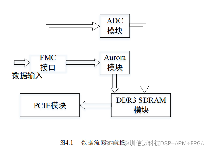
Among them, the ADC module is the driver for the AD daughter card, providing a sampling rate of 1 GSa/s and a data resolution of 12 bits. The Aurora module is the driver for the optical fiber daughter card, using the Aurora protocol, with 4 channels, a single-channel rate of 10 Gbps, and a total rate of 40 Gbps. The PCIe interface uses the PCIe 2.0 protocol, x8 mode, with a single-channel rate of 5.0 Gbps, and a total rate of 40 Gbps. The DDR3 SDRAM module is used to cache Aurora or ADC data. Vivado software provides IP cores for Aurora, PCIe, and MIG, offering interface solutions for the Aurora protocol, PCIe protocol, and DDR3 SDRAM, respectively. The detailed design of each module is described below.
4.2.2 ADC Module Logic Design
The maximum sampling rate of the ADC chip on the AD daughter card is 1.6 Gsps. In the performance analysis in Chapter 2, the ADC's sampling rate must not be lower than 706.6 MSa/s. In this design, the ADC's sampling rate is set to 1 GSa/s.
The ADC chip operates in dual-edge sampling mode, allowing the sampling rate to be twice the sampling clock. A 500 MHz differential clock signal needs to be generated. The MMCM resources within the Zynq chip can generate a 500 MHz single-ended clock, and then the OBUFDS primitive provided by Xilinx is used to convert the single-ended clock into a differential clock output.
Since the ADC operates in dual-edge sampling, the DES pin of the ADC chip needs to be pulled high. The signal coupling method is AC coupling, requiring the VCMO pin to be set to low. In dual-edge operating mode, the ADC chip can select multiplexing mode, which allows for data line reuse. The timing diagram for multiplexing mode is shown in Figure 4.2 [25].
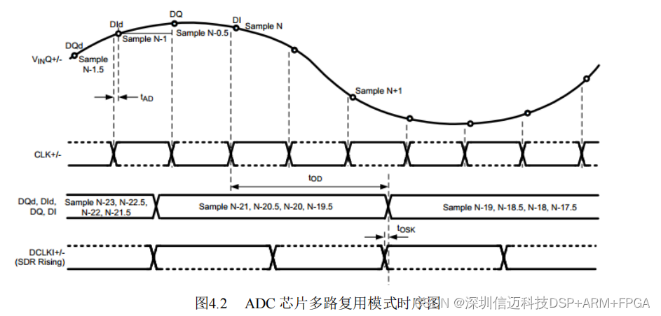
In the figure, CLK+/- are the sampling clock signals, DQd, Did, DQ, DI are the ADC data lines, and DCLKI+/- is the data synchronization output clock for channel I. As can be seen from the figure, when the ADC operates in dual-edge sampling and multiplexing mode, after 4 conversions, data is sequentially output to DQd, Did, DQ, DI. Simultaneously, a divided-by-two conversion clock signal is output on DCLK+/-, which is 250 MHz here.
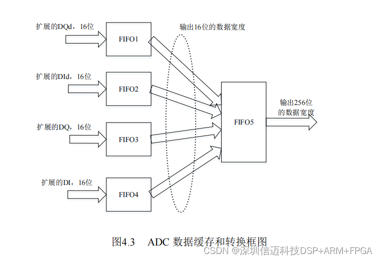
Since the data bit width is 12 bits, but the FIFO width of the DDR3 SDRAM module is 256 bits, they are not integer multiples of each other. The solution here is to extend the 12-bit data from each data channel to 16 bits, then save them separately into smaller FIFOs, and finally use one FIFO to output a 256-bit data width. The data flow buffering block diagram is shown in Figure 4.3. Among them, FIFO1~FIFO4 are synchronous FIFOs with both read and write widths of 16 bits. The FIFO clock is the DCLK+/- clock from the ADC chip, after differential-to-single-ended conversion. The data output from the 4 FIFOs is written into FIFO5. FIFO5 is an asynchronous FIFO with a write data width of 64 bits and a read data width of 256 bits, which can be directly connected to the DDR3 SDRAM module.
The optical fiber interface uses the Aurora protocol, with 4 channels, a single-channel rate of 10 Gbps, and a total rate of 40 Gbps. Data transmission for the optical fiber interface is implemented based on the Aurora protocol IP core provided by Vivado software. This IP core offers two types: 8B/10B and 64B/66B, corresponding to their respective encoding schemes. This design uses 64B/66B encoding, which increases bandwidth utilization. The IP core instantiation process is shown in Figure 4.4.
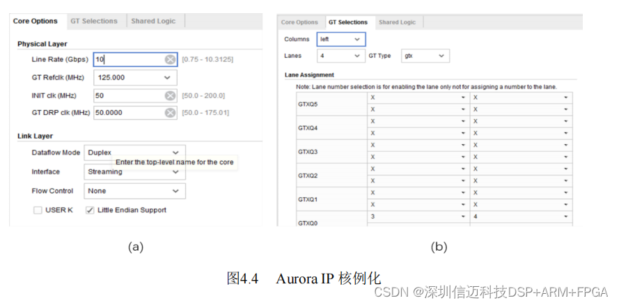
When instantiating the core, the transmission rate is first specified, set to 10 Gbps here. According to the hardware circuit design, the reference clock here is set to 125 MHz, and transmission uses full-duplex streaming mode for ease of design and use. Then, the channel mapping on the chip is specified.
The instantiated core is shown in Figure 4.5.