Design of a High-Speed PCIe Data Acquisition Card Based on ZYNQ (3) Hardware Design
Acquisition Card Hardware Design
3.1 Introduction
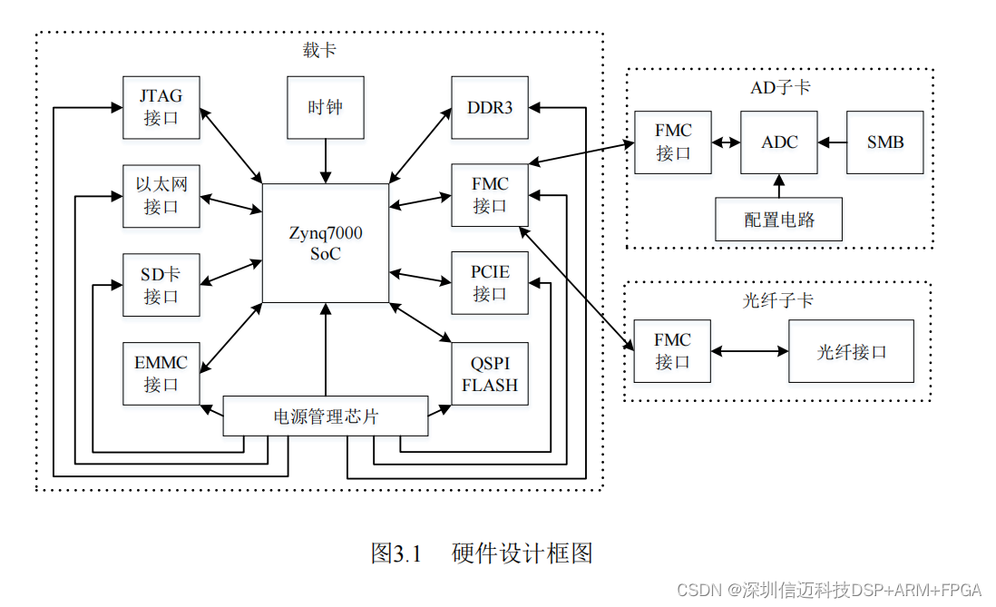
Hardware design of the acquisition card is the foundation for realizing data acquisition functions. A well-designed hardware platform facilitates easier implementation of acquisition functionality and simplifies software development. This chapter provides a detailed description of the hardware design of the acquisition card based on the hardware architecture outlined in Chapter 2, including component selection, configuration, and specific circuit designs for both the carrier card and daughter cards. The overall hardware block diagram of the carrier and daughter cards is shown in Figure 3.1.
3.2 Carrier Card Hardware Design
3.2.1 Main Control Chip Selection and Configuration Circuit
(1) Main Control Chip Selection and Analysis
Based on the hardware design analysis presented in Chapter 2, the control chip must meet the following requirements:
- The chip must include high-speed GTX interfaces, with no fewer than 12 differential pairs (4 pairs for optical fiber, 8 pairs for PCIe).
- Sufficient on-chip BRAM resources must be available to serve as FIFO buffers.
- The chip must support both Aurora and PCIe 2.0 protocols.
- The chip should have peripheral interfaces to facilitate debugging and ensure good portability.
Considering these requirements, the Xilinx Zynq-7000 series SoC is selected as the main control chip. The product categories and PL-side resources are listed in Table 3.1 [23].
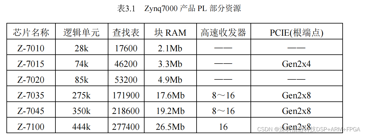
As shown in Table 3.1, Zynq-7135 and lower-end models meet the design requirements of this acquisition card. After comparative analysis, the XC7Z100FFG900-2 from the Zynq-7100 series is selected. This device integrates a Processing System (PS) with dual ARM Cortex-A9 cores and a Programmable Logic (PL) section based on the Xilinx Kintex-7 FPGA architecture.
3.3 Daughter Card Circuit Design
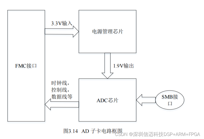
3.3.1 ADC Daughter Card Circuit Design
The ADC daughter card performs analog-to-digital conversion of input signals and transmits the digitized data to the Zynq chip on the acquisition card via the FMC interface.
The ADC chip selected is the ADC12D800 from Texas Instruments, which supports a maximum sampling rate of 1.6 GSPS with a resolution of 12 bits. Depending on configuration, the conversion results can be output either as 12 differential pairs or in parallel as separate data lines. The ADC supports dual-channel data conversion—designated as I and Q channels—each with independent data outputs. The chip supports both single-edge and double-edge sampling, with its operating mode controlled through clock and control interfaces.
The chip's clock and control interface signals and their functions are listed in Table 3.5.
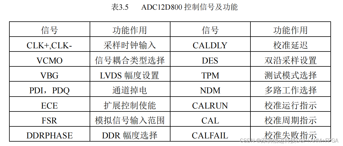
The ADC also features an SPI bus interface, which can be used to configure the device—such as for biasing and calibration—when operating in extended control mode. Since the current design does not utilize the SPI bus, further details on SPI configuration methods and register functions are not discussed here.
The ADC uses differential voltage input. In this design, analog signals are AC-coupled into the ADC chip. After entering through an SMB RF connector, the signal is converted into two differential signals before being fed into the ADC. The corresponding circuit schematic is shown in Figure 3.13.
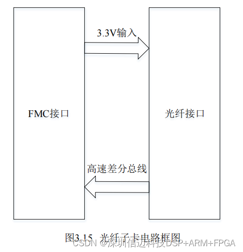
3.3.2 Optical Fiber Daughter Card Circuit Design
The optical fiber daughter card provides an interface conversion from optical fiber to the FMC connector. The fiber interface uses the 1761987-9 QSFP connector, which provides four high-speed differential lanes and is typically used with optical modules, offering a compact and high-speed transmission solution.
The optical transceiver used in this design is the SR4-40G module, supporting a data rate of 40 Gbps with a transmission distance of up to 150 meters. The optical interface requires a 3.3V power supply, which is provided by the acquisition card through the FMC interface. The four high-speed differential signal pairs are routed directly to the FMC connector. The block diagram of the optical fiber daughter card is shown in Figure 3.15.