Design of a ZYNQ-Based PCIe High-Speed Data Acquisition Card (2): System Architecture and Host Software
Overall Design of the Acquisition Card and Related Technologies
2.1 Introduction
This project originates from a radar emitter identification system, requiring the acquisition, transmission, and storage of intermediate frequency (IF) signals from radar emitters. Based on project requirements, this chapter presents the overall design scheme of the data acquisition card. The design encompasses both hardware and software components. First, the performance specifications of the acquisition card are analyzed. Then, the overall hardware architecture is proposed, followed by the software architecture built upon the hardware design. Finally, relevant protocols and key technologies used in the system are explained.
2.2 Overall Design Overview
2.2.1 Analysis of System Specifications
In this project, the IF signal bandwidth of the radar emitter ranges from 760 MHz to 1060 MHz. This radar signal is a bandpass signal. Applying the bandpass sampling theorem allows for a reduced sampling rate, thereby lowering the data transmission rate and simplifying both hardware and software implementation.
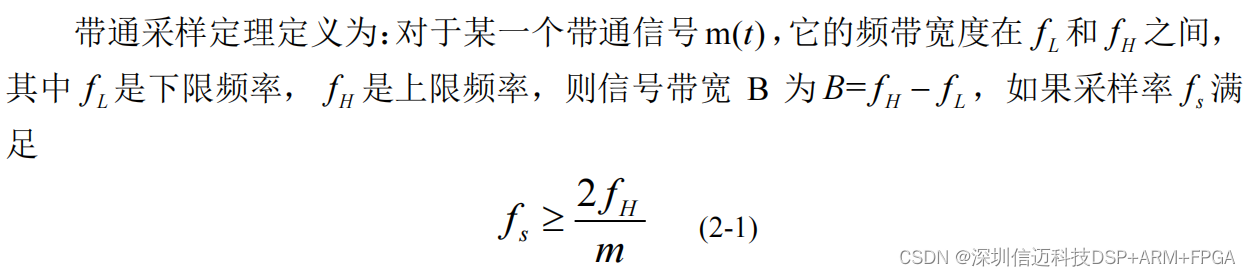
The original signal can thus be reconstructed from the sampled values, where m is the largest integer not exceeding
From Equation 2-1, a sampling rate greater than 706.6 Msa/s is sufficient to reconstruct the original radar emitter signal from the sampled data. However, in practice, due to non-ideal filter characteristics, an excessively low sampling rate may cause spectral aliasing, resulting in poor signal reconstruction quality. Therefore, the actual sampling rate must exceed the theoretical minimum to ensure acceptable signal fidelity. The AD daughterboard in this design supports a maximum sampling rate of 1.6 Gsa/s with 12-bit resolution, yielding a maximum data rate of 19.2 Gbps, meeting the project's data acquisition requirements.
The sampled data forms a high-speed data stream that enters the processor via a high-speed interface, requiring an efficient and stable processor and high-speed data transfer protocol to handle data reception, processing, and transmission. The Zynq-7000 series SoC integrates an FPGA-based programmable logic (PL) section and an ARM-based processing system (PS) section on a single chip, enabling integrated data acquisition and processing. The AD daughterboard designed in this project performs analog-to-digital conversion of radar signals and delivers the resulting high-speed data stream to the acquisition card.
Due to varying high-speed interface types, protocols and transfer rates differ. A direct connection approach may lead to data loss. In certain cases, a minimum amount of data is required before processing can begin, necessitating a data buffering mechanism. DDR3 SDRAM chips are commonly used for high-speed data buffering. DDR3 SDRAM supports data read/write operations on both clock edges. Current DDR3 SDRAM chips support a maximum clock frequency of 800 MHz. With a 16-bit data bus width, a single DDR3 chip can theoretically achieve a maximum read/write rate of 25.6 Gbps. In practice, multiple DDR3 chips are used in combination to increase both data capacity and bus width, while also proportionally improving data throughput. Considering miniaturization, this design employs two 16-bit DDR3 SDRAM chips on both the PL and PS sides of the Zynq chip, forming a 32-bit-wide buffer.
The high-speed interface in this design uses PCIe. To meet the radar signal data rate requirement of at least 19.2 Gbps, the PCIe interface must support a comparable or higher rate. After analysis, PCIe 2.0 in x8 mode is selected, providing a data transfer rate of 40 Gbps, which satisfies the project's data transmission needs.
2.2.2 Hardware System Design
Based on the analysis in the previous section, this section presents the overall hardware design. The hardware architecture and data flow diagram are shown in Figure 2.1:
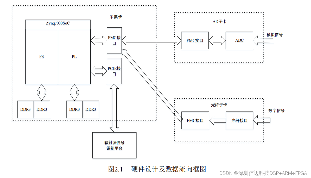
For design flexibility, the acquisition system adopts a carrier board + daughterboard architecture, connected via the FMC interface, enabling compatibility with various daughterboards. The carrier board follows a module + baseboard design: the module contains the minimal system of the Zynq-7000 SoC, with chip interfaces routed through connectors to the baseboard, which primarily provides power and connects peripheral interfaces of the Zynq-7000 SoC. To support diverse application scenarios, the system supports two data acquisition and transmission methods: an optical fiber daughterboard and an AD daughterboard. The optical fiber daughterboard receives high-speed digital signals, while the AD daughterboard performs analog-to-digital conversion of emitter signals, generating a high-speed data stream. The high-speed data output from either daughterboard enters the Zynq chip via the FMC interface and is then transmitted via PCIe to the radar emitter signal identification platform for further processing.
The AD daughterboard uses an SMB RF connector for analog signal input and employs the ADC12D800 ADC chip from Texas Instruments. This ADC supports a maximum sampling rate of 1.6 Gsa/s with 12-bit resolution. The digitized data is output via 12 differential parallel buses using LVDS signaling. The chip supports dual-channel analog input and double data rate (DDR) sampling. The ADC signal lines are routed to the FMC interface for easy connection to the carrier board. Similarly, the optical fiber daughterboard routes optical interface signals to the FMC interface to enable system integration.
2.2.3 Software System Design
The acquisition card software system consists of three parts: FPGA logic design, embedded software design, and host software design. The FPGA logic design focuses on module implementation and inter-module data exchange. Embedded software development involves kernel porting of the Zynq-7000 SoC on a virtual machine. The host software handles PCIe device detection and initialization, data reception, and file storage for subsequent processing. The detailed design is as follows.
(1) FPGA Logic Design Overview
The logic design is developed using the Vivado 2017.4 platform. Vivado is a design suite developed by Xilinx specifically for the 7-series devices. It includes the SDK tool, enabling embedded development for Zynq-7000 SoCs.
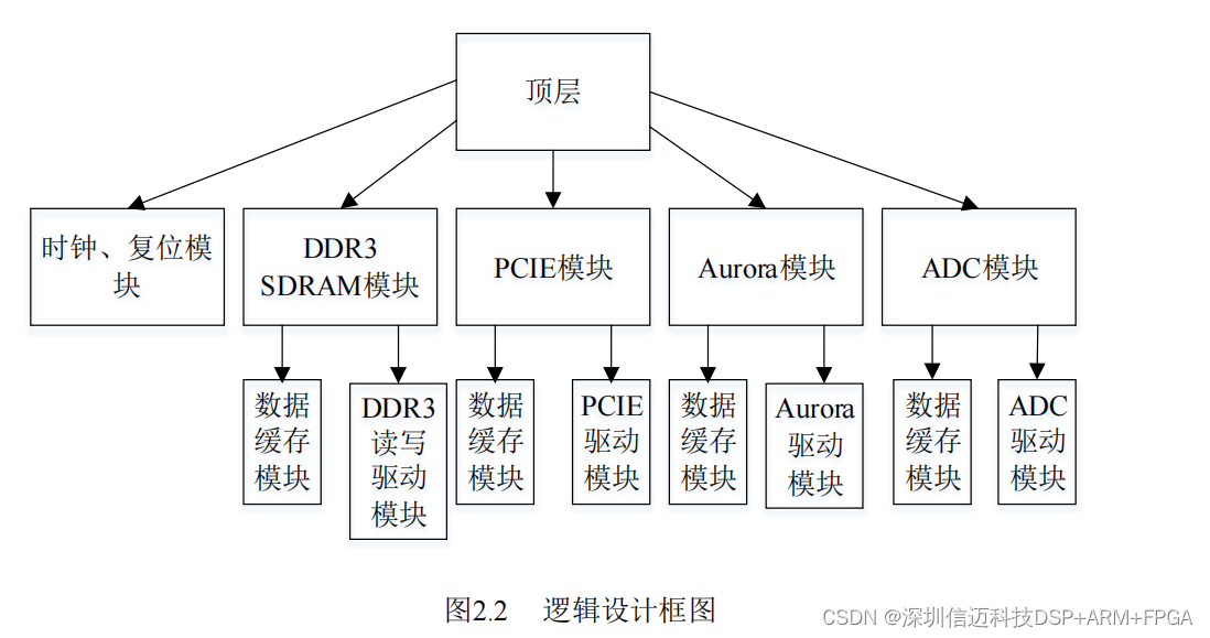
A top-down design methodology is adopted. The design involves several protocols: Aurora, DDR3 SDRAM interface, and PCIe, each implemented as a separate module. Aurora is a fiber-optic communication protocol used for receiving and forwarding optical data. The DDR3 SDRAM interface module handles initialization and read/write operations for high-speed data buffering. The PCIe module manages data exchange between the acquisition card and the radar emitter identification platform. Vivado provides a rich set of IP cores, offering ready solutions for high-speed interface protocols and DDR3 SDRAM.
Due to differing clock domains among these protocols, modular design is essential. Direct inter-module connections may lead to data loss due to lack of synchronization. To address this, asynchronous FIFOs are used. Asynchronous FIFOs have independent read and write clocks, and their data widths can be set in integer multiples, providing greater design flexibility. The overall logic design comprises five modules:
- Clock and reset module: provides clock and reset signals to all modules.
- DDR3 SDRAM module: implements high-speed data buffering.
- PCIe module: includes PCIe driver functionality for data exchange between the acquisition card and the host PC.
- Aurora module: serves as the optical fiber driver, handling data reception and forwarding.
- ADC module: configures and drives the ADC chip, enabling radar signal digitization and data forwarding.
Except for the clock and reset module, each module consists of a driver sub-module and a data buffering sub-module. The data buffer is implemented as a FIFO interface to facilitate inter-module connectivity. The logic design block diagram is shown in Figure 2.2.
To meet the project's requirement of a data transfer rate no less than 19.2 Gbps, and considering the FMC interface's maximum data rate of 10 Gbps per lane, the optical fiber interface uses four lanes, each operating at 10 Gbps, achieving a total rate of 40 Gbps. To maintain synchronization with the optical link, PCIe 2.0 with x8 configuration is used, providing a per-lane rate of 5.0 Gbps and a total bandwidth of 40 Gbps—matching the optical interface rate. This transfer rate adequately supports most high-speed data transmission scenarios.
(2) Embedded Software Design Overview
Embedded software development primarily targets the PS side and prepares the system for future user applications. Based on the completed PL design, the embedded development is carried out using Vivado's built-in SDK platform under a Linux environment. This design is implemented on Ubuntu, where a series of script files are executed for system compilation, kernel building, image generation, and image flashing.
(3) Host Software Design Overview
The host software must be capable of identifying, detecting, and initializing the acquisition card, receiving data from the PCIe interface, and saving the data to files.
Developing a PCIe driver on a PC requires a driver development tool. This project uses WinDriver, a driver development platform developed by Jungo. WinDriver supports multiple operating systems and provides the windrvr.sys kernel module, enabling core-level interaction with the OS. This allows developers to avoid direct kernel programming and instead use function libraries for kernel communication, significantly simplifying driver development and improving efficiency.
The host software is developed using Microsoft's Visual Studio (VS), a multi-language development platform. The design leverages WinDriver's kernel and API libraries to achieve PCIe device initialization and data exchange. Due to variations in CPU performance across different PCs, interrupt response and data processing capabilities differ. Therefore, DMA (Direct Memory Access) is typically used for data transfer. Setting an appropriate DMA transfer length allows the CPU to operate at peak efficiency. The DMA length can be configured either in the FPGA logic or by the host software. For practicality and flexibility, setting the DMA length via the host software is preferred.
Based on the above analysis, the host software must provide the following functions:
- PCIe device open, close, and initialization;
- DMA transfer length configuration;
- Data saving and file generation.