Design of a High-Speed PCIe Data Acquisition Card Based on ZYNQ (Part 1)
As the first step in information processing, data acquisition is becoming increasingly important. Currently, data acquisition has been widely applied in aerospace, civilian, military, and medical fields. With continuous advancements in related technologies, signal frequencies are rising and bandwidths are expanding, driving data acquisition technology toward high-speed, large-volume data processing. In electronic warfare applications, the emergence of various complex wideband radar systems has made electromagnetic signals in space more complicated. To identify specific signals within such complex electromagnetic environments, high-speed ADCs are first required to sample the electromagnetic signals, followed by high-speed data transmission to a processor for further processing and analysis, thereby extracting information embedded in the signals. Typically, high-speed data acquisition cards perform the tasks of signal acquisition and transmission, while data processing can either be completed by a high-performance processor on the card itself or the data can be stored and later processed by a PC.
Currently, common processors include FPGA, ARM, DSP, and PowerPC, most of which provide high-speed serial interfaces to enable fast data transfer. High-speed serial interfaces transmit data via multiple differential pairs, offering stronger noise immunity and higher speeds compared to traditional parallel buses, effectively avoiding crosstalk and synchronization issues inherent in parallel bus architectures [1]. Processors such as ARM and DSP are based on CPU architectures and can execute only one instruction at a time. In contrast, FPGAs are digital circuit-based chips where different modules operate independently, giving FPGAs unparalleled parallel processing capabilities compared to ARM or DSP processors [2]. However, FPGAs are less suitable for complex data processing tasks and are typically paired with ARM or DSP for such purposes.
Typically, data acquisition cards adopt an FPGA+ARM or FPGA+DSP architecture, where the FPGA handles signal acquisition and data transmission, while the ARM or DSP performs data processing. This separation of processing functions increases circuit design complexity, and software development requires different platforms, resulting in longer development cycles. This design employs the Zynq-7000 series SoC as the main control chip, which integrates an FPGA+ARM architecture within a single chip [3]. This integration simplifies circuit design and allows both FPGA and ARM functionalities to be developed on a single platform, significantly reducing development time. Data acquisition cards commonly use Ethernet or PCIe interfaces. Ethernet offers relatively low transmission speeds and is unsuitable for high-speed data transfer, whereas PCIe can easily achieve transmission rates of tens of Gbps, making it widely adopted in high-speed data acquisition cards.
This project addresses the high-speed data acquisition requirements of radar emitters by designing and implementing a high-speed PCIe data acquisition card. The Zynq-7000 SoC is used as the processing chip, and the PCIe 2.0 protocol enables data exchange between the acquisition card and the radar emitter signal identification platform. DDR3 SDRAM is employed for data buffering, achieving a maximum data transfer rate of up to 40 Gbps. This design provides a practical approach and implementation method for high-speed signal acquisition and transmission, offering meaningful insights and reference value.
1.2 Research and Development Status at Home and Abroad
1.2.1 Status of High-Speed Data Acquisition Cards
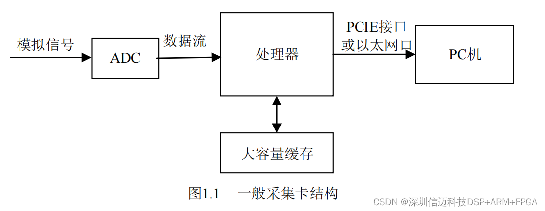
A typical high-speed data acquisition card adopts the structure shown in Figure 1.1. After analog signals are sampled by an ADC, they are sent to a processor. The data is then buffered and processed before being transmitted to a computer via a PCIe or Ethernet interface. The processor usually employs an FPGA+DSP or FPGA+ARM architecture. In this setup, the FPGA handles data acquisition, while the DSP or ARM performs data processing. Large-capacity buffers typically use DDR2 or DDR3 chips for temporary data storage. Alternatively, sampled data can be directly transferred to a PC via a high-speed PCIe interface for subsequent processing. High-speed data acquisition relies heavily on advances in high-speed ADCs and high-speed bus technologies. The following sections provide a detailed overview of the current state of ADC development and processor architectures.