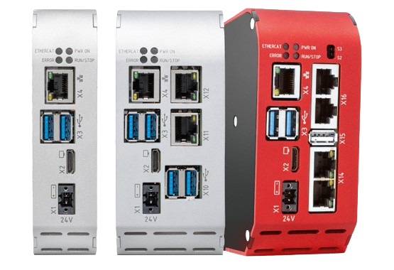
Low-Cost ARM+FPGA+Codesys Soft PLC Solution Based on AM62x
Introduction to GPMC Parallel Interface
GPMC (General Purpose Memory Controller) is a unique general-purpose memory controller interface specific to TI processors. It supports 8/16-bit data width, provides up to 128MB of addressable space, and operates at a maximum clock rate of 133MHz. GPMC is the dedicated interface used in processors such as AM62x, AM64x, AM437x, AM335x, and AM57x for connecting to external memory devices, including:
(1) FPGA devices
(2) ADC devices
(3) SRAM memory
(4) NOR/NAND flash
Three Key Features of GPMC Parallel Interface
(1) Small Data – Low Latency
In industrial automation applications such as industrial PLCs, integrated drive and control units, motion controllers, CNC mainboards, relay protection equipment, and small-current grounding line selection systems, precision and speed are critical. The "small data – low latency" characteristic of the GPMC parallel interface stands out, significantly improving data transfer efficiency and reducing transmission costs.
(2) Big Data – High Bandwidth
The era of big data imposes higher requirements on data transmission and processing in the energy and power sectors. GPMC offers maximum flexibility by supporting different timing parameters and data width configurations across four configurable chip selects. Optimal chip select settings can be applied based on the characteristics of the connected peripheral. By configuring GPMC interface timing parameters and operating modes, data rates exceeding 100MB/s can be achieved. Thus, the "big data – high bandwidth" feature of GPMC plays a vital role in energy and power applications.
(3) Low Cost – Low Power Consumption
"Low cost, low power, high performance" is a prevailing trend in intelligent devices. Compared to PCIe serial interfaces, the GPMC parallel interface offers lower cost and reduced power consumption. While both are commonly used communication interfaces capable of meeting high-speed communication needs, users often prefer GPMC when interfacing with FPGAs because:
- High-speed communication can be achieved using low-cost FPGAs, whereas FPGAs with PCIe interfaces are significantly more expensive.
- FPGAs with PCIe interfaces typically consume more power, while low-cost FPGAs have lower power requirements. In general, low-power devices also tend to have longer operational lifespans.
CPU Direct Access Method
Taking AM62x as an example, when connected to an FPGA via the GPMC interface using CPU direct access, write speeds of up to 15.501MB/s and read speeds of up to 5.744MB/s can be achieved.
This method is suitable for "small data – low latency" scenarios.
Program Flow Description:
(1) The ARM side writes data to the FPGA BRAM via the GPMC bus;
(2) The ARM side reads data from the FPGA BRAM via the GPMC bus;
(3) Verify the correctness of the written and read data, and calculate the read/write throughput.
UDMA-Based Access Method
Using AM62x as an example, when connected to an FPGA via the GPMC interface using UDMA, write speeds of up to 73.90MB/s and read speeds of up to 77.47MB/s can be achieved. In practice, by tuning GPMC timing parameters and operating modes, maximum transfer rates can exceed 100MB/s.
This method is suitable for "big data – high bandwidth" scenarios.
Note: Due to limitations and interference from cabling during testing, the measured bit error rate may be higher than expected.
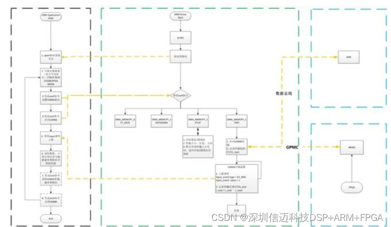
Program Flow Description
ARM Side:
(1) Use UDMA mode;
(2) Write data into a contiguous memory space allocated by the dma_memcpy driver (located in DDR);
(3) Configure UDMA parameters such as source address, destination address, and data size;
(4) Write operation: Initiate UDMA via the ioctl function to transfer data from DDR to FPGA BRAM over the GPMC bus;
(5) After receiving an input event reported by the driver, use the ioctl function to retrieve the data transfer duration and calculate the UDMA write throughput;
(6) Read operation: Initiate UDMA via the ioctl function to transfer data from FPGA BRAM to the contiguous memory space allocated by the dma_memcpy driver;
(7) After receiving the input event from the driver, copy the data from kernel space to user space, verify data integrity, and use the ioctl function to obtain transfer duration and calculate UDMA read throughput.
FPGA Side:
(1) Parse data according to the GPMC timing from the ARM side and access internal FPGA BRAM resources. The BRAM has a 10-bit address width, 16-bit data width, and a total memory size of 2KB (1024 × 16-bit).
Codesys Tutorial Background
In the previous tutorial, we completed the connection and configuration of the controller device. This tutorial continues with the HK-MC-Prime as an example, assuming the controller is already configured and connected to the developer's PC, demonstrating how to install the appropriate version of CODESYS V3 and create your first program.
- Installing CODESYS
(1) Choosing the Appropriate Version
It is important to note that controllers cannot work with arbitrary versions of CODESYS V3. The required CODESYS V3 version and corresponding target depend on the controller's firmware version. Therefore, it is crucial to install a compatible version of CODESYS V3 for your specific controller rather than using the latest version of the CODESYS V3 development environment directly.
To find the controller's firmware version, refer to the previous tutorial's section "Configuration via Web Interface," log into the controller's web interface, and open the "System Info" page.
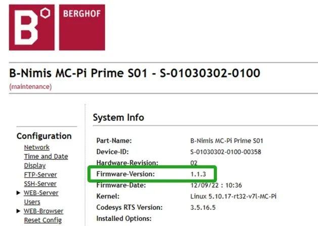
As shown in the image above, the controller's firmware version is 1.1.3, and the HK-MC-Prime is based on the Pi control platform. According to the compatibility table between firmware versions and CODESYS V3 versions, the required development environment for this controller is: CODESYS 3.5.16.50. You can download the corresponding installation package from the CODESYS official website.
(2) Installing CODESYS V3
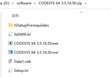
As shown in the image above, after downloading the installation package, follow these steps to install CODESYS V3:
- Start Installation
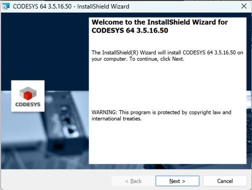
Run the file CODESYS.3.5.16.50 as an administrator to begin the installation process.
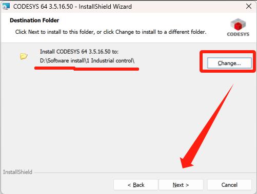
- Customize Installation Location
Click "Next," accept the license agreement, then click "Next" again to proceed to the following screen, where you can customize the software installation directory:
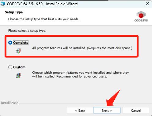
- Select Features
If you are unsure which features you need, perform a complete installation of all components. Otherwise, you may deselect unnecessary features.