NI USB9218 Domestic Counterpart: 51.2 kS/s/ch, 2-Channel C Series Universal Analog Input Module
51.2 kS/s/ch, 2-Channel C Series Universal Analog Input Module
The NI‑9218 is designed for multi-purpose measurements. It provides built-in support for accelerometers, powered sensors, full-bridge and voltage measurements, as well as quarter-bridge, half-bridge, 60V, and current measurements using adapters tailored for specific measurements. Each channel is individually selectable, allowing users to perform different measurements on each channel. The NI‑9218 is an ideal choice for developing universal test systems required for automotive, off-highway, and data logging applications.
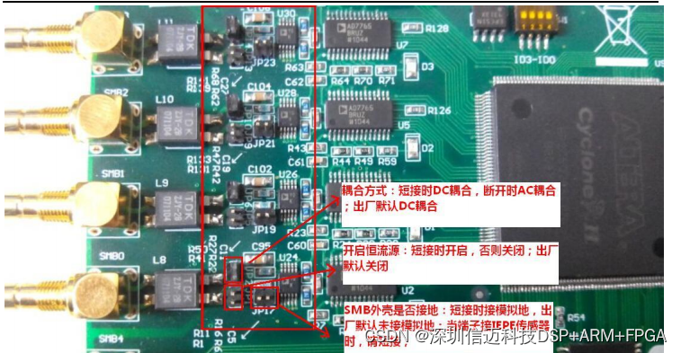
III. Product Applications The XM-USB-4431 is a data acquisition card based on the USB2.0 bus, which can be directly connected to a computer's USB port to form data acquisition, waveform analysis, and processing systems in various fields such as laboratories and product quality inspection centers. It can also be used to build industrial production process monitoring systems. Its main application areas include: • Sound/Vibration Signal Acquisition and Analysis • Electronic Product Quality Inspection • Medical Testing • High-Precision Synchronous Signal Acquisition • I/O Control IV. Performance Features • A/D Converter: 24-bit Σ-Δ type ADC: AD7765 (optional support for 312KSPS AD7764) • Low intrinsic noise, high channel isolation; • Differential input range: ±10V; • Independent programmable gain, 4 adjustable levels: 1x, 10x, 100x, and 1000x; • AD Trigger Modes: Software timed trigger, external trigger; • Supports pre-trigger, with a maximum pre-acquisition of 2K points; • IEPE Constant Current Source: 4.38mA @2% (the board may require an external 5V power supply, depending on the USB port's power capability); • IEPE Sensor Excitation Voltage: 15V or 24V; • Constant Current Source Output Impedance: >250 kΩ at 1kHz; • Constant Current Source Noise: <500 pA/√Hz; • Coupling Mode: AC/DC; • AC Coupling -3dB Cutoff Frequency: 0.53Hz; • Analog input signal with TVS clamp protection function; • Sampling frequency can be set by software (range: 1.95KHz~156.25KHz); • Onboard large-capacity memory (4M words), supports continuous acquisition for real-time monitoring; • Onboard EEPROM, users can write custom parameters; • Board ID recognition (0~15), supports multi-card operation; • 8-channel DI/DO; outputs with latching function, automatically cleared upon power-up; • Provides drivers and dynamic link libraries for WIN7/VISTA/2000/XP; • Dimensions (excluding enclosure): 91(W) × 139(L) (mm); V. Technical Parameters • Operating Voltage: 5V±0.25V • Operating Temperature: 0℃~70℃ • Storage Temperature: -10℃~85℃ • Humidity: 5%~95% VI. Working Principle 6.1 Logic Block Diagram
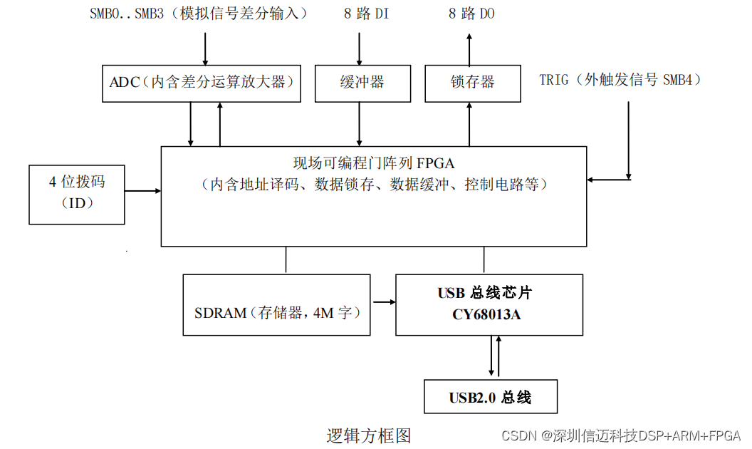
6.2 Brief Description of Working Principle The XM-USB-4431 consists of the following functional modules: USB2.0 bus bridge circuit, address decoding and data latching, AD conversion, data storage, and other functions. Address Decoding and Data Latching: Controlled by a Field-Programmable Gate Array (FPGA) chip. Since it uses the USB2.0 bus, users do not need to concern themselves with specific I/O addresses; they can directly call the dynamic link library provided by our company. In 8-bit data mode, the specific I/O addresses are interpreted by the USB master control chip. AD Conversion: External analog signals are input via SMB0..SMB3, pass through 4 levels of programmable gain, and then enter the ADC. The AD control timing is completed by the FPGA. Data Storage: The results of AD conversion are stored in SDRAM. The timing for reading and writing data is controlled by the FPGA. Digital I/O: 8 channels of digital input, 8 channels of digital output. Outputs have a latching function and are automatically cleared upon power-up. Frequency Measurement Principle: Measures the interval between two adjacent rising edges of a signal (square wave). For example: the software sends a measurement command, and the system clock (4MHz) is used to measure the interval between two adjacent rising edges of the signal under test. The interval is expressed as the number of system clock cycles, allowing users to easily calculate the signal's frequency. Since the maximum interval is represented by 24-bit data (maximum 0xFFFFFF, i.e., 16777215), the maximum timing length is 4.19S (16777215 * 0.25 µs ≈ 4.194303S).
Description: When the START signal is low, the software initiates a frequency measurement, measuring the time width between two adjacent rising edges of the signal under test (which is 5 system clock cycles, with a system clock of 4MHz). In the diagram, the TimerOver signal indicates: 1: frequency measurement not finished; 0: frequency measurement finished. The frequency of the external signal is calculated as Fre = 4 × 10^3 ÷ (XCounter), in KHz.