Development and Experimental Verification of a Multi-type Synchronous Signal Acquisition Instrument Based on ARM+FPGA+AD Platform (Part Two) Overall Board Design
2.2 Overall Board Design
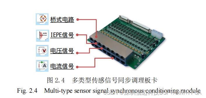
This chapter develops a multi-type sensor signal synchronous conditioning board based on AD7193+RJ45, as shown in Figure 2.4. It is responsible for converting analog electrical signals from sensors into digital signals for acquisition by the data acquisition system. It achieves the functions of free switching of sensor signal types in a single channel and synchronous acquisition of multiple types of sensor signals (including bridge circuit signals, IEPE sensor signals, current, and voltage, a total of four types of sensor signals).
This module has the following functions:
(1) Conditions bridge circuit signals, IEPE sensor signals, voltage, and current sensor signals, converting these four types of sensor signals into 0~2.5V voltage signals;
(2) Free switching of the acquired sensor signal type within a single channel;
(3) Synchronous acquisition of signals from each channel;
(4) Possesses hardware-level filtering and noise reduction functions.
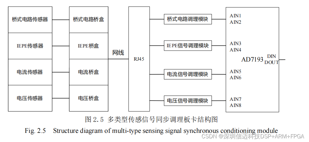
The board includes 16 AD conversion and conditioning channels. The structure of each conversion and conditioning channel is shown on the right side of the network cable in Figure 2.5, including an RJ45 interface, bridge circuit, IEPE signal, current and voltage signal conditioning modules, and an AD7193 chip. The RJ45 interface serves as the sensor signal input interface, and the pin slots extended from the digital pins of the AD7193 chip are used for data acquisition system operations. The board is powered by a 6-wire power interface, which provides 5V, 12V, and 24V voltages.
Functional Module Design of the Acquisition Instrument
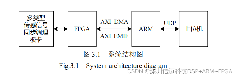
This paper develops a multi-type synchronous signal acquisition instrument based on the ZYNQ platform. Through a flexible system division of labor model, it achieves precise synchronous acquisition of multiple types of sensor signals (voltage, current, bridge, and IEPE). The system structure is shown in Figure 3.1, comprising the following four parts:
The first part is the multi-type sensor signal synchronous conditioning board, which includes 16 AD conditioning and conversion channels, converting analog electrical signals into digital electrical signals, and realizing conditioning, free switching, and synchronization of multiple types of sensor signals. This has been introduced in Chapter 2.
The second part is the FPGA-side data acquisition unit, responsible for acquiring 16-channel AD data from the multi-type sensor signal synchronous conditioning board and realizing data interaction with the ARM side via AXI DMA and AXI EMIF.
The third part is the ARM-side data transmission unit, responsible for data interaction with the FPGA side and interacting with the host computer using the UDP protocol.
The fourth part is the host computer, which interacts with the ARM side via UDP protocol and performs system configuration, completing data visualization and local storage functions.
This chapter will specifically introduce the core part of the entire multi-type synchronous signal acquisition system – the ZYNQ system. It includes two parts: the FPGA-side data acquisition unit and the ARM-side data transmission unit. The following will introduce four aspects: the system board of the acquisition system, the overall design scheme and related protocol technologies, the design of the FPGA-side data acquisition unit, and the design of the ARM-side data transmission unit.
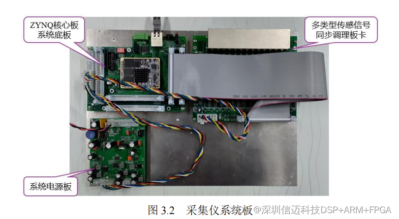
3.1 System Board
The system board of the acquisition instrument includes the Punctual Atom ZYNQ core board, the system baseboard, the system power board, and the multi-type sensor signal synchronous conditioning board. The remaining pins are used to expand 4 AD boards. The system board is shown in Figure 3.2.
Xinmai provides ARM+FPGA+AD localized solutions