ARM + FPGA GPIB IP Core Implementation
Currently, Tektronix and Agilent, both US companies, are leaders in data generator technology.
Agilent's family of benchtop pulse/data generators offers a maximum clock frequency of 3GHz (timing generator). The E81200 data generator achieves a data rate of 660Mb/s with 8 channels, meaning it can produce waveform outputs up to 330MHz.
Tektronix's typical benchtop data generator, the Tek DG2020A, has a clock frequency of 200MHz and can produce graphical data output at 100MHz, featuring powerful waveform editing software. Data patterns can be generated using the data pattern editor, which includes capabilities such as graphical editing, timing waveform sequence combination editing, and table editing. Some domestic universities and research institutions are dedicated to developing data generators, with some capable of producing 100M programmable digital signals. However, due to shortcomings in product design and manufacturing processes, they have not yet formed commercial data generator products.
This paper will focus on the GPIB interface design for high-speed data generators. It proposes two solutions for implementing the GPIB communication interface hardware: using a dedicated chip (NAT9914) and using an FPGA. Coupled with corresponding interface software drivers, this will facilitate easy integration of the instrument with other equipment for automated system testing.
2.1 Main Operating Principles of High-Speed Data Generators
A high-speed data generator consists of hardware and software. The following outlines the overall hardware and software architecture and its main operating principles.
The entire hardware system is centered around an embedded computer for functional definition and module partitioning. It primarily comprises an embedded computer, clock unit, trigger unit, pattern data generation unit, output unit, panel control and display, and communication interfaces. As shown in Figure 2-1.
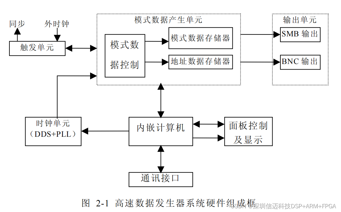
The clock unit is implemented using DDS+PLL, forming the foundation for the entire high-speed data generator's operation. Its main function is to generate an internally continuous frequency-adjustable clock signal. The pattern data generation unit consists of three components: the pattern data control circuit, pattern data memory, and address data memory. Among these, the pattern data control circuit is the core of the entire unit, controlling the simultaneous multi-channel output of data and the sequential switching of serial data. It is designed using dedicated ASIC circuits, and high-speed SRAM is used for data storage. The trigger unit is used for outputting synchronous clocks and transforming external clocks. The BNC output circuit comprises three parts: the analog circuit section (i.e., level information processing), the digital circuit section (i.e., frequency information processing), and the final stage driver section (information synthesis output). The communication interface circuit includes interfaces such as Ethernet, serial port, and GPIB. The Ethernet and serial ports are built into the embedded computer, while the GPIB interface is implemented using an FPGA or a dedicated chip.


3.2.5 Selection of Design Chip
This design uses ALTERA's FPGA chip ACEX1K30QC208 for implementation.
The 1K30 chip belongs to ALTERA's ACEX series, which is a family of FPGA devices launched by ALTERA for applications in communications, audio processing, and similar fields. It uses a 0.22/0.18 micron hybrid process, with densities ranging from 10,000 to 100,000 gates. It still employs ALTERA's traditional LUT (Look-Up Table) combined with EAB (Embedded Array Block) structure. The chip includes an embedded array that can implement memory and dedicated logic functions, supporting single and dual-port RAM modes. An IOE (I/O Element) contains a bidirectional I/O buffer and a register, and can be configured as an input, output, or bidirectional pin.
The ACEX1K30QC208 has a maximum system gate count of 30,000 gates, 1728 logic macrocells, and 6 embedded system blocks. It can provide up to 24567 RAM bits, with 208 pins. Excluding configuration and power pins, the actual usable pin count is 141, which fully meets the design requirements. [8]
Once the circuit design is finalized, it is written into a configuration EPROM. Upon each power-up, it is loaded into the FPGA to realize the designed circuit functionality.
3.3 Specific Design Implementation of the System
3.3.1 Overall Framework
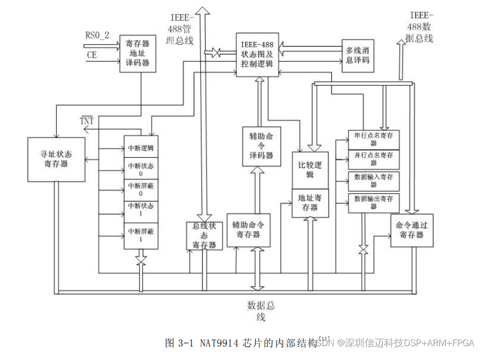
To ensure a certain degree of generality, the GPIB interface design for the high-speed data generator primarily references the internal structure of the NAT9914 chip, as shown in Figure 3-1. We divide the entire system to be designed into several basic functional module units. The implementation of these basic units is done using a language-based description, which not only facilitates future portability across development environments but also greatly simplifies functional debugging and localized modifications.
We can divide the entire system into several subsystems. These include the control logic for the microprocessor's ISA interface, the interface functions for communicating with the GPIB bus, and the data channel section. The design of each subsystem can also be broken down into module-level designs, which provides strong flexibility during debugging and system assembly, and also facilitates code debugging and reuse.
The control logic for the ISA interface will be detailed in Chapter 4. Since the chosen FPGA chip, ACEX1K30QC208, has a sufficient number of logic macrocells, this part can be downloaded into the FPGA chip, eliminating the need for an additional EPM3128ATC100-10. As this section will be elaborated on in detail later, it will not be repeated here.
The design of the interface functions is the core of the design, being both a key focus and a challenge. It requires not only a deep understanding of the IEEE488 protocol but also specific requirements for the selection of the interface function subset.
The data channel section includes a register file and combinational logic circuits. The internal registers of the data channel consist of 13 registers, of which 11 are selected as needed, including read-only and write-only registers. They serve as the data bridge between the microprocessor and the GPIB interface function. The design of this subsystem is also a key focus.
After completing the basic modules, graphical symbols can be generated for each module. When assembling the entire system, these symbols can be directly invoked in a manner similar to drawing circuit diagrams, making the design relatively intuitive and providing a comprehensive understanding of the overall system-level architecture. After completing the "software" design of the entire internal circuit, the next step is to concretely embed this "software core" (CORE) onto the specifically selected FPGA, typically by downloading it via the JTAG port.
3.3.2 Implementation of Interface Function State Machine
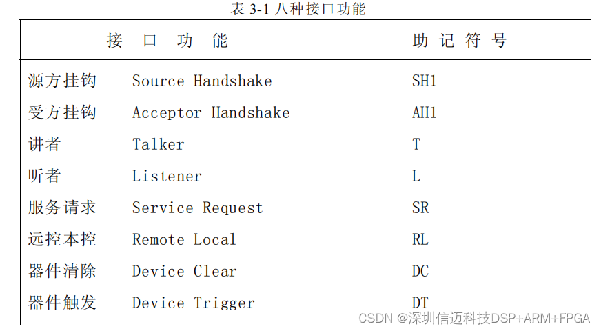
According to the requirements of the high-speed data generator, eight interface functions were selected for the design: Source Handshake, Acceptor Handshake, Talker, Listener, Service Request, Remote/Local, Device Clear, and Device Trigger. Each interface function is divided into several related states, allowing for the introduction of state machine design when implementing these interacting state transitions using Verilog HDL.
I. Introduction to State Machines
[12]
Finite State Machines (FSMs) can be classified in different ways from various perspectives.
Based on the determinism of state transitions, FSMs can be divided into deterministic finite state machines and non-deterministic finite state machines. Based on the trigger conditions for state transitions, they can be divided into synchronous state machines and asynchronous state machines. Synchronous state machines' trigger conditions are limited to a predetermined time and signal (e.g., system clock signal), and changes in input signals do not immediately cause corresponding state changes. Asynchronous state machines undergo state transitions and produce corresponding outputs whenever input signals change. In terms of complexity, there are single FSMs and communicating state machines. Communicating state machines can be further divided into master-slave communicating state machines and concurrent communicating state machines. From the perspective of input-output functional relationships, single FSMs can be classified into Mealy-type and Moore-type finite state machines, which represent the most common classifications of finite state machines.
● Mealy State Machine and Moore State Machine
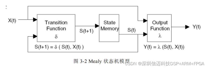
- Mealy State Machine
The output of a Mealy state machine is a function not only of the current state but also of the current input. Figure 3-2 shows the model of a Mealy state machine.
- Moore State Machine
The output of a Moore state machine is solely a function of the current state, independent of the current input X(t). Therefore, a Moore state machine is a special case of a Mealy state machine. Figure 3-3 shows the model of a Moore state machine.
Generally, Mealy-type state machines have fewer state variables, which means using fewer state storage elements. In practical engineering applications, Mealy state machines are mostly adopted. Moore-type state machines are easier for algebraic analysis, and in the algebraic theory of FSMs, Moore-type state machines are often used as the object of study.
II. Selection of Interface Functions
The IEEE488-1975 standard specifies ten interface functions, each operating according to specific protocols. Based on the specific requirements of the instrument, we selected eight interface functions, as shown in Table 3-1.