Design of a VME Bus Controller Based on RK3399 + FPGA (Part 2): Hardware and FPGA Logic Design
3.2 FPGA Minimal System Design
An FPGA minimal system refers to the most basic system required for the FPGA to operate properly, including power circuits, configuration circuits, clock, and reset circuits. The FPGA used in this design is the PG2L100H from TsingMicro. The following sections detail the circuit design of each component in the FPGA minimal system.
(1) Power Circuit Design
The FPGA requires multiple power supply voltages: 3.3V, 1.8V, 1.2V, and 1V. Specifically, the core logic and dedicated RAM (DRAM) modules use 1V; the auxiliary power supply is 1.8V; the IO BANKs use 3.3V; and the HSST high-speed serial interface requires both 1V and 1.2V analog supplies. The FPGA power design block diagram is shown in Figure 3-5 below.
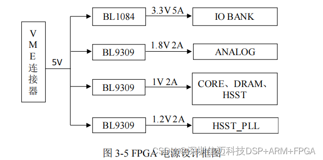
The input 5V power is converted using Shanghai Belling's power chips BL1084 and BL9309.
BL1084 is an LDO regulator that provides a fixed 3.3V output with a maximum output current of up to 5A.
BL9309 provides an adjustable output voltage; resistive dividers are used to generate 1V, 1.2V, and 1.8V supplies, with a maximum output current of 2A.
(2) Configuration Circuit Design
The PG2L100H supports multiple configuration modes. This design uses JTAG mode and Master SPI mode.
The JTAG interface allows programming to be downloaded into the FPGA's internal SRAM or permanently stored into external Flash.
In Master SPI mode, the program is stored in an external SPI Flash, and the FPGA actively reads the bitstream from the Flash upon power-up.
This design uses GigaDevice's SPI Flash as the external configuration device for the FPGA. The Flash model is GD25Q32CSIGR, with a capacity of 32Mb, which meets the design requirements.
(3) Clock and Reset Circuit Design
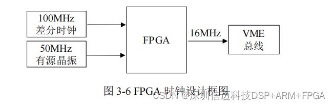
FPGAs are clock-driven devices, making clock and reset circuits essential. This design uses a 50MHz active crystal oscillator from Shenzhen Yangxing Technology as the system clock input for the FPGA, connected to the FPGA's global clock pin. Internally, the 50MHz clock is divided by a phase-locked loop (PLL) to generate a 16MHz clock, which is then output to the VME bus connector. Additionally, the FPGA’s PCIe interface requires a 100MHz differential reference clock, which is provided by the RK3399 processor. The FPGA clock design block diagram is shown in Figure 3-6 below.
The FPGA's power-on reset signal comes from the RK808-D. However, since the RK808-D outputs a 1.8V logic level while the FPGA's IO level is 3.3V, level translation is required. A level translator chip from Jiangsu Runshi is used for this conversion. In addition, a manual reset button is provided for the FPGA to perform a user-initiated reset.
3.4 VME Interface Circuit Design
As an embedded controller board, communication with other functional boards must be achieved through a computer bus. The controller designed in this project must ultimately operate within a VME test system, so a VME interface circuit must be implemented.
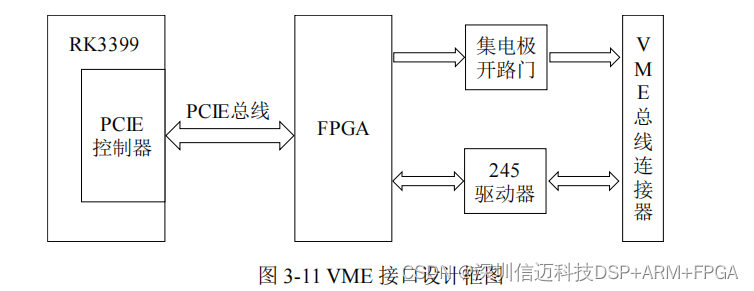
Since the RK3399 processor does not include a built-in VME controller, the interface logic between PCIe and the VME bus must be implemented independently. As the VME bus interface is realized through FPGA logic, the PCIe interface on the RK3399 is connected to the FPGA. The RK3399 controls the VME bus by reading and writing registers inside the FPGA via the PCIe bus. The VME interface design is illustrated in Figure 3-11.
The VME bus interface is implemented through cooperation between FPGA logic and driver circuits, with the FPGA handling the conversion between the PCIe and VME interfaces. Since the FPGA’s IO voltage is 3.3V while VME bus signals operate at 5V, a driver circuit is required for level translation. A 245 bidirectional driver from Jiangsu Runshi is used to perform level conversion between the VME connector and the FPGA.
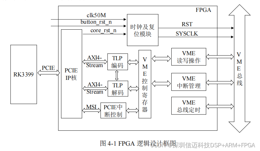
FPGA logic design involves using Verilog HDL or VHDL to implement the required digital logic circuits. In this project, the FPGA logic design primarily implements the interface conversion between the PCIe and VME buses. This chapter details the design in two main parts: PCIe interface logic and VME interface logic.
4.1 FPGA Logic Design Overview
The FPGA logic primarily implements the interface conversion from the PCIe bus to the VME bus. The logic design block diagram is shown in Figure 4-1, consisting mainly of PCIe interface logic and VME interface logic. Internal registers for controlling the VME bus are implemented within the FPGA. The RK3399 controls the VME bus by reading and writing these registers via the PCIe bus.
4.2 PCIe Interface Logic Design
The PCIe interface logic, implemented using Xilinx’s PCIe IP core on the TsingMicro FPGA platform, enables communication between the RK3399 processor and the FPGA. The RK3399 acts as the PCIe Root Complex (RC), while the FPGA acts as the PCIe Endpoint. CPU addresses are mapped to the PCIe device's BAR0 and BAR1 memory spaces. BAR1 is used to access VME bus addresses, while BAR0 is used for reading and writing control registers.
The PCIe IP core complies with the PCIe 2.1 specification, supports link widths of x1, x2, and x4, and link speeds of 2.5GT/s and 5GT/s. The PCIe IP implements the transaction, data link, and physical layers of the PCIe protocol and provides AXI4-Stream interfaces for data transfer between the application layer and transaction layer.
The PCIe interface logic includes the PCIe IP core, TLP decoding module, TLP encoding module, PCIe interrupt control module, clock and reset logic, address mapping, and control register design. TLP (Transaction Layer Packet) consists of a header and optional data. TLP decoding and encoding are implemented using the AXI4-Stream interface—a parallel bus without address lines, using valid and ready handshake signals for data transfer. The PCIe IP provides both AXI4-Stream Master and Slave interfaces, allowing users to design custom TLP decoding and encoding logic.
4.2.1 TLP Decoding Module Design
The TLP decoding module receives TLPs from the PCIe IP and parses them to extract address and data information. The TLP header is either 3 or 4 DWORDs (DW) long. The 3DW header format for memory read/write requests is shown in Figure 4-2. Fields marked "R" are reserved and must be set to 0 [42].
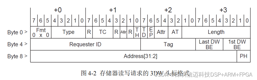
The Fmt and Type fields define transaction characteristics. TC (Traffic Class) indicates the transmission class, with eight levels (TC0–TC7) defined by PCIe; TC0 is the default. The Attr field is 3 bits wide: bit 2 indicates support for ID-based ordering, bit 1 for relaxed ordering, and bit 0 for cache coherency requirements. In this design, Attr[2:0] is set to 000, indicating default (strong) ordering and automatic cache coherency via bus snooping. Under strong ordering, transactions of the same type must complete sequentially, while different transaction types may be processed out of order.
The Length field specifies the TLP data payload size in DW units. The 1st DW BE and Last DW BE fields indicate byte enables for the first and last DWs, respectively—0 means the byte is invalid, 1 means valid.
The Tag field determines how many TLPs of the same type the PCIe transmitter can queue. Typically, only the lower 5 bits are used (supporting up to 32 TLPs). If Extended Tag is enabled, 8 bits are used (supporting up to 256 TLPs). Since memory write requests do not require completion packets, the Tag field is set to 0. Address[31:2] provides the 32-bit memory address; the lower 2 bits are reserved (00b), enforcing DW alignment.
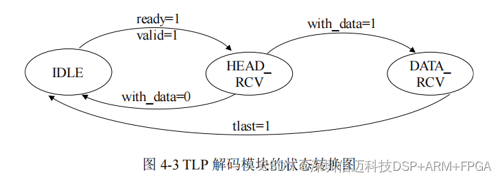
The TLP decoder uses an AXI4-Stream Master interface and is implemented via a finite state machine (FSM). Figure 4-3 shows the state transition diagram.
The TLP decoding FSM has three states: IDLE, HEAD_RCV, and DATA_RCV. The initial state is IDLE, where all registers (e.g., address, data) are cleared after reset. When both ready and valid signals are high, data transmission begins, and the state transitions to HEAD_RCV. In HEAD_RCV, the TLP header is received and parsed to extract the transaction type and address. If with_data is 1, the transaction is a memory write (with data), so the state transitions to DATA_RCV. If with_data is 0, it's a memory read (no data), and the state returns to IDLE. In DATA_RCV, the TLP data is received. When tlast is asserted (high), data transfer completes, and the state returns to IDLE to await the next TLP.
Additionally, the AXI4-Stream Master interface includes an 8-bit tuser signal, where bits [6:4] indicate which BAR the TLP targets.
4.2.2 TLP Encoding Module Design
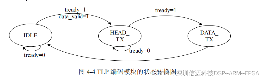
The TLP encoding module packages data and address from the VME bus into TLPs and sends them to the PCIe IP via the AXI4-Stream Slave interface. Figure 4-4 shows the state transition diagram for TLP encoding.
The TLP encoding FSM includes three states: IDLE, HEAD_TX, and DATA_TX. The initial state is IDLE. If tready is 0, the RC is not ready, and the state remains IDLE. When tready and data_valid are both high, the state transitions to HEAD_TX. In HEAD_TX, the TLP header fields are assembled. Since completion TLPs have a fixed 3DW header, a 3DW header is formed and sent to the PCIe IP, with tready set high to indicate valid data. When tready is high, the state transitions to DATA_TX, where the completion data is transmitted (tready remains high). After data transmission, the state returns to IDLE and tready is set low.
4.2.3 PCIe Interrupt Control Design
PCIe supports two types of interrupts: Message Signaled Interrupts (MSI) and virtual INTx interrupts. MSI interrupts are generated when a PCIe device performs a memory write to a specific address defined by its message address register, carrying interrupt data. Virtual INTx interrupts emulate traditional PCI INTx# signals using interrupt messages to convey signal transitions.
MSI interrupts are more efficient because they eliminate the need for software to identify the interrupt source. Therefore, this design uses MSI interrupts, which are enabled in the PCIe IP configuration interface. When an interrupt is received from the VME bus, the MSI interrupt request signal is asserted, and the PCIe IP forwards the request to the CPU’s PCIe controller. After the CPU processes the interrupt, it deasserts the MSI request signal to prevent duplicate interrupts.
When using MSI interrupts, memory synchronization must be considered. The CPU may begin executing the interrupt handler immediately upon receiving the MSI, potentially interrupting ongoing memory operations. To avoid this, ensure that the TC (Traffic Class) of the MSI memory write transaction matches that of the application data write transaction, preventing preemption.
4.2.4 Address Mapping and Control Register Design
CPU addresses are mapped to the PCIe device’s BAR0 and BAR1 memory spaces. BAR0 is used for control register access, while BAR1 is used to access VME bus addresses. Since the VME bus has 24 address lines, BAR1 is configured as 16MB. Based on actual register usage, BAR0 is set to 256B. These settings are configured within the PCIe IP core.
To control the VME bus, several control registers are defined and mapped to the PCIe device’s BAR0 space. The VME control registers defined in this project are listed in Table 4-1. Since PCIe memory space accesses are DWORD-aligned, all register addresses are multiples of 4.
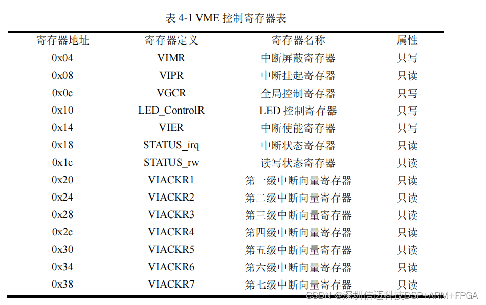
These registers fall into two categories: interrupt control and read/write control.
Interrupt control registers include interrupt mask, interrupt pending, interrupt enable, interrupt vector, and interrupt status registers. The interrupt mask register allows selective disabling of specific interrupt levels. The interrupt pending register indicates which interrupt level has been triggered. The interrupt enable register enables or disables VME interrupts. The interrupt vector register provides the interrupt vector for handling. Both the mask and pending registers are 8 bits wide, with bit 0 unused.
Read/write control registers include the global control register, read/write status register, and LED control register. The global control register configures the address mode (16-bit or 24-bit) and data access mode (16-bit, 8-bit even address, or 8-bit odd address). The read/write status register indicates the outcome of VME bus operations: 1 = write completed, 2 = read completed, 4 = data access mode error, 8 = timeout error. The LED control register controls front-panel LEDs, turning them on after power-up.
The VME control register module acts as a bridge between the PCIe and VME interfaces, enabling PCIe-to-VME interface conversion. It maps PCIe addresses from the TLP decoding module to BAR0 and BAR1 spaces, allowing read/write access to VME control registers in BAR0 and VME data in BAR1. It also passes register contents, VME data, and addresses to the VME read/write operation module and VME interrupt management module. Note that if a VME bus read/write operation is not complete, the system must wait until completion before initiating the next operation.
4.3 VME Interface Logic Design
The VME bus is an asynchronous parallel bus consisting of four main parts: the Data Transfer Bus (DTB), arbitration bus, priority interrupt bus, and common bus. The DTB transfers data, addresses, and control signals between modules. The arbitration bus manages DTB access, ensuring only one module controls it at a time. The priority interrupt bus enables interrupt requests and responses between VME devices and the interrupt manager, supporting seven interrupt priority levels.
The DTB includes address lines, data lines, and control lines. The VME backplane can be configured with either 16 or 32 data lines. A 16-line backplane transfers 2 bytes per cycle; a 32-line backplane transfers 4 bytes. DTB control lines include AS*, DS0*, DS1*, DTACK*, WRITE*, and BERR*. A falling edge on AS* indicates valid address strobing. The first falling edge of DS0*/DS1* indicates valid data on the bus during a write cycle, or signals the slave to release data during a read cycle. WRITE* is active low for master-to-slave data transfer and high for slave-to-master. BERR* is driven low by the slave or bus timer to indicate a data transfer error.
The VME interface logic in this project includes the VME read/write operation module, VME interrupt management module, VME timing module, clock driver, and reset logic. The clock and reset logic generates the 16MHz VME system clock (via PLL division) and reset signals (via a reset button). The following sections detail the design of the read/write operation, interrupt management, and timing modules.
4.3.1 VME Read/Write Operation Module
This module controls data transfer on the VME bus, supporting three data access modes. The design principle is asynchronous data transfer via handshake signals. The VME controller uses AS*, DS0*, and DS1* to send control signals, while the VME slave responds with DTACK*.
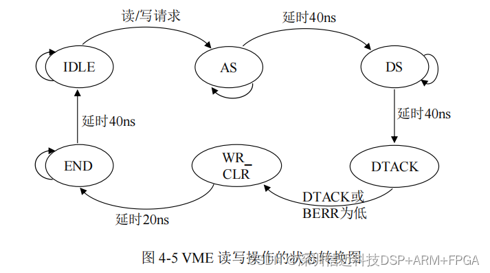
The read/write module is implemented as a finite state machine (FSM), with the state transition diagram shown in Figure 4-5. The initial state is IDLE. When a read/write request is received and the bus is free, the state transitions to AS (Address Strobe). If the bus is busy, it remains in IDLE. In AS, after a 40ns delay, AS is driven low and WRT is asserted, transitioning to DS (Data Strobe). After another 40ns delay in DS, DS signals are driven based on the data access mode, and the state transitions to DTACK (Data Transfer Acknowledge). If DTACK is low, the transfer succeeds; AS and DS are deasserted, and the state transitions to WR_CLR (Write Clear). If BERR is low, a timeout error occurred; AS and DS are still deasserted, and the state transitions to WR_CLR. In WR_CLR, after a 20ns delay, the WRITE signal and read/write flags are cleared, transitioning to END. After a 40ns delay in END, the state returns to IDLE.
4.3.2 VME Interrupt Management Module
This module receives and processes interrupts IRQ1 through IRQ7. When an interrupt is received, it performs interrupt acknowledgment and forwards the information to the PCIe interrupt control module, which then issues an MSI interrupt request to the RK3399. The RK3399 reads the interrupt pending and vector registers to determine the interrupt level and type. The process is as follows:
(1) Upon receiving a VME interrupt request (IRQ), the VME interrupt management module writes the interrupt level to the corresponding pending register and forwards the interrupt to the PCIe interrupt module.
(2) The PCIe interrupt control module issues an MSI interrupt request to the RK3399.
(3) The RK3399 enters the interrupt handler, disables further interrupts, reads the pending register to identify the active interrupt level (1–7), and reads the interrupt vector for processing.
(4) After the RK3399 reads the interrupt vector, the VME register control module sends an IACK_en signal to the VME interrupt module, enabling acknowledgment.
(5) The VME interrupt module drives IACK* low and reads the interrupt vector from the VME functional module, passing it to the register control module.
(6) After the application completes interrupt handling, the RK3399 writes to the interrupt enable register, signaling that the interrupt has been processed and the system is ready for the next one.
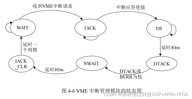
The state transition diagram for the VME interrupt module is shown in Figure 4-6. The initial state is WAIT. Upon receiving an interrupt, it forwards the interrupt and transitions to IACK (Interrupt Acknowledge). In IACK, if the acknowledgment enable signal is received (indicating the processor is ready), the module performs acknowledgment and transitions to DS. In DS, after a 40ns delay, DS and AS are driven active, transitioning to DTACK. In DTACK, when DTACK or BERR goes low, IACK, AS, and DS are deasserted, transitioning to NWAIT. After a 40ns delay in NWAIT, the state transitions to IACK_CLR, indicating completion. After one cycle, it returns to the initial state.
4.3.3 VME Timing Module
The VME timing module implements a 64μs timeout. If the VME bus operation exceeds 64μs, BERR* is driven low to signal a timeout error. Two timing methods exist:
(1) If either DS0* or DS1* remains low for more than 64μs (regardless of DTACK* or BERR*), BERR* is driven low.
(2) If either DS0* or DS1* remains low for more than 64μs and both DTACK* and BERR* are high, BERR* is driven low.
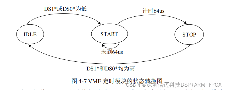
This design uses method (2), implemented via a state machine for 64μs timing. The FSM has three states: IDLE (initial), START (timing begins), and STOP (timing ends). The state transition diagram is shown in Figure 4-7.
After reset, the system is in IDLE. When either DS0* or DS1* goes low, the state transitions to START and timing begins. The state transitions to STOP when DTACK* goes low or when 64μs elapses. If the timeout condition is met, BERR* is driven low. If neither condition is met, the state remains in START. When both DS0* and DS1* are high, the state returns to IDLE and BERR* is driven high.
The VME timing module handles bus timeouts and errors. When the controller accesses an undefined address or a VME functional module fails, the module reports the error and terminates the operation, improving bus efficiency.
Xinmai provides RK3399 + FPGA solutions.