[Domestic Virtual Instrument] Multi-channel Synchronous Data Acquisition Design Scheme Based on ZYNQ7045+V7 FPGA (Part 2)
The main process of the multi-channel data acquisition circuit is to achieve 4-channel analog signal reception, with data undergoing analog-to-digital conversion and signal processing before being transmitted via optical fiber to the central station. The multi-channel data acquisition circuit consists of an analog signal acquisition unit, a digital signal processing unit, and a signal adapter board. The block diagram is shown in Figure 4-1.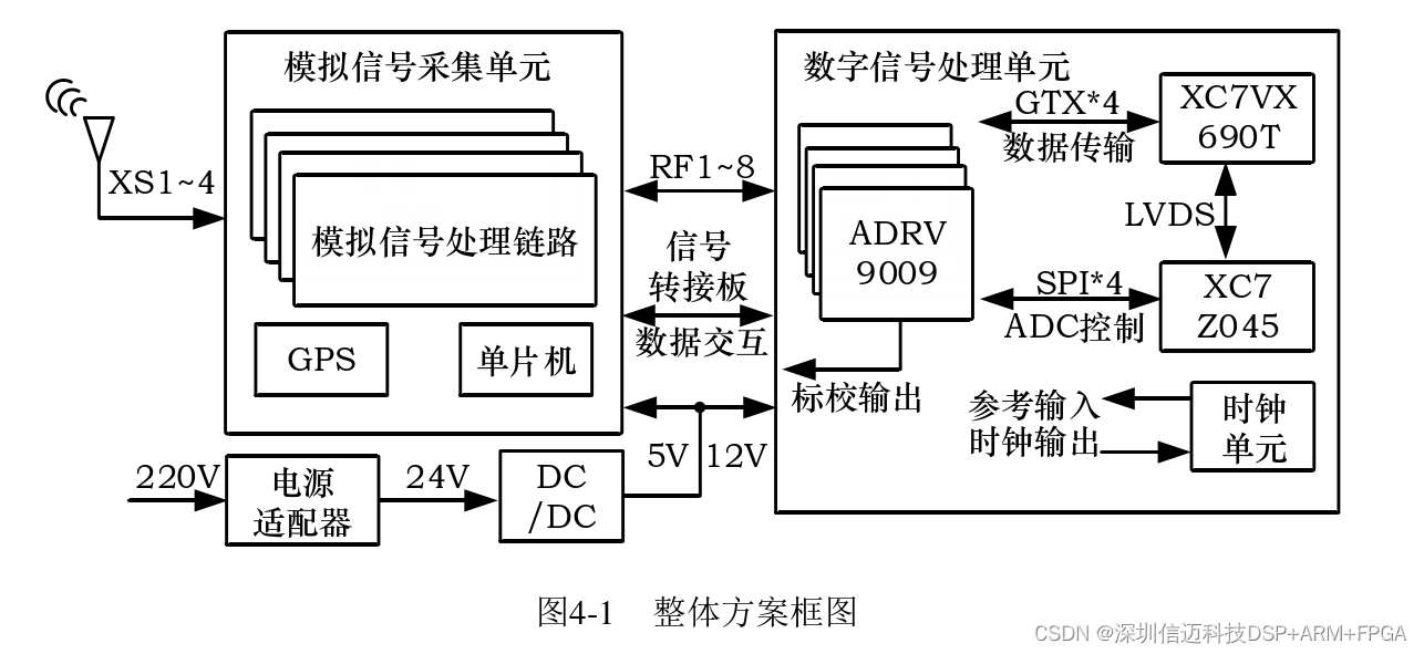
To perform reconnaissance and monitoring of multiple key frequency points within the bandwidth, the digital signal processing unit utilizes 8 receiver channels from 4 ADRV9009 analog-to-digital converter chips. The 4-channel analog signal processing circuit is divided into 8 paths connected to the 8 inputs of the ADCs, enabling a single ADC to focus on monitoring two key frequency points within the bandwidth. Each frequency point has 4 synchronous reception paths, which reduces signal processing complexity and improves computational accuracy.
The digital signal processing unit integrates one XC7Z045 and one XC7VX690T to provide circuit control and digital signal processing capabilities. The signal adapter board primarily handles power connections, signal interconnection, and functional expansion between the analog signal acquisition unit, the digital signal processing unit, and the power module. The power module converts AC 220V to DC 24V and supplies power to each unit via DCDC+LDO mode.
The acquisition and processing flow for a single channel signal is shown in Figure 4-2. The analog signal undergoes filtering, amplification, and power division by the analog signal acquisition circuit before entering the ADRV9009 analog-to-digital converter chip. After passing through the ADRV9009's built-in LNA, the built-in Local Oscillator (LO) performs zero-IF conversion of the analog signal. Subsequently, the I/Q modulation module completes phase conversion to output two I/Q signals, which are then sampled by the ADC. Finally, the resulting I/Q signals are output to the XC7VX690T after passing through an FIR filter.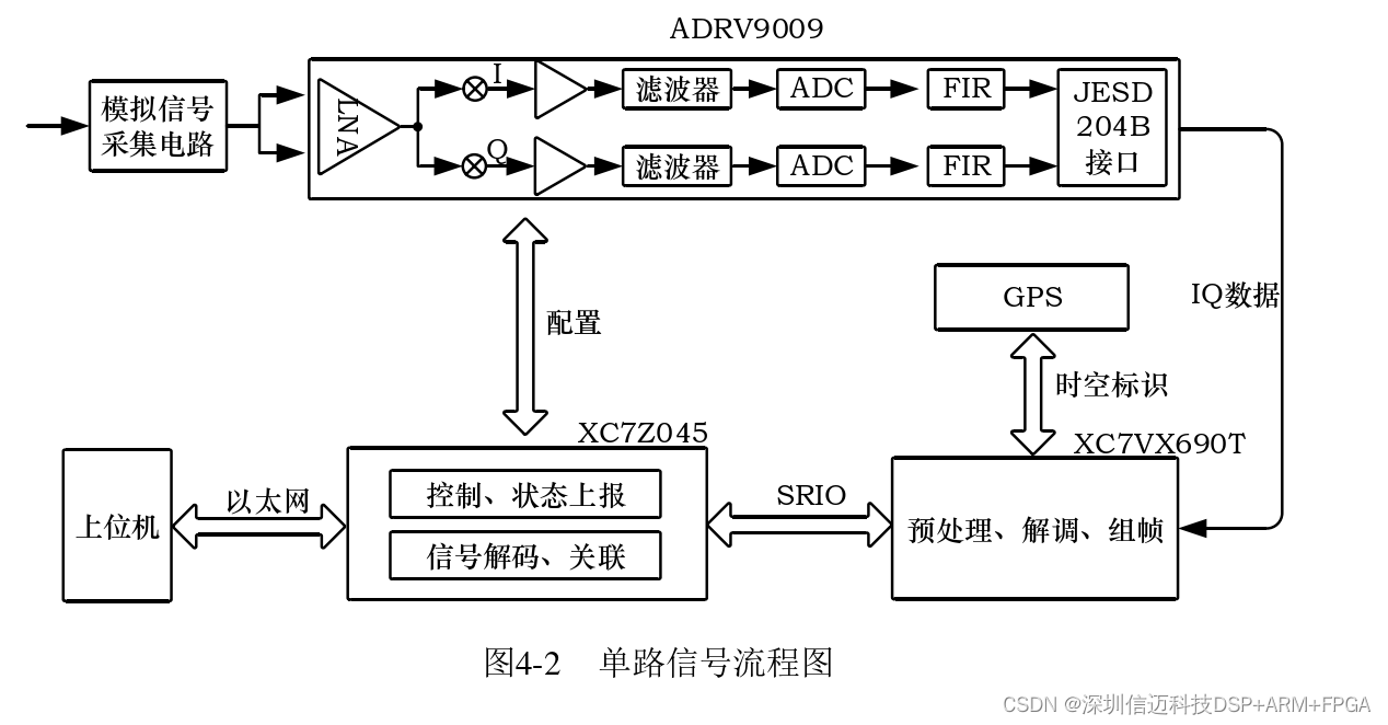
After the data reaches the XC7VX690T, it undergoes further pre-processing, demodulation, and framing. The data information is then transmitted to the XC7Z045 via a RapidIO interface. The XC7Z045 performs signal decoding, sorting, and correlation operations, and then transmits the processed results or full pulse parameters to the host computer for analysis and processing via a Gigabit Ethernet interface. The XC7Z045 serves as the control hub for the entire receiver chain, managing the analog signal acquisition unit and the digital signal processing unit. It adjusts the bandwidth of the input channel filters, controls gain modes and levels, tunes the output of the ADRV9009's local oscillator, and adjusts sampling rates at various stages.
4.2 Analog Signal Acquisition Circuit Design 4.2.1 Design Block Diagram The principle design block diagram of the analog signal acquisition unit is shown in Figure 4-3.
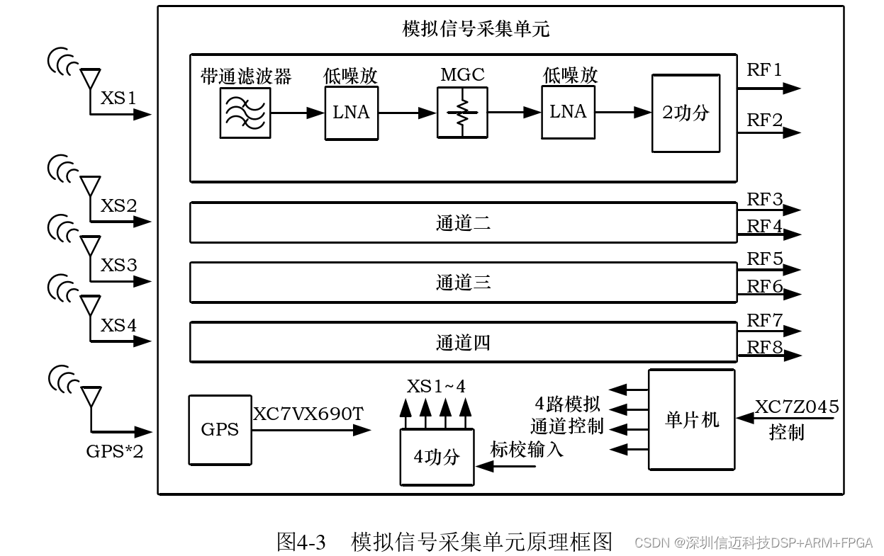
The analog signal acquisition unit pre-selects 4 analog signals, providing filtering, gain, and coupling correction functions. These are then power-divided into 8 analog signals and fed into the digital signal processing unit. An integrated GPS receiver timestamps the output data and provides positioning and north-finding capabilities. A microcontroller configures the analog signal processing chip. Interconnection with the digital signal processing unit via an adapter board enables the XC7Z045 to control the microcontroller and the XC7VX690T to analyze GPS signals. 4.2.2 Analog Signal Acquisition Circuit Design The analog signal acquisition circuit includes 4 conditioning channels, primarily for receiving 4 signals in the 700MHz-1600MHz band. The block diagram for a single analog signal chain is shown in Figure 4-4.
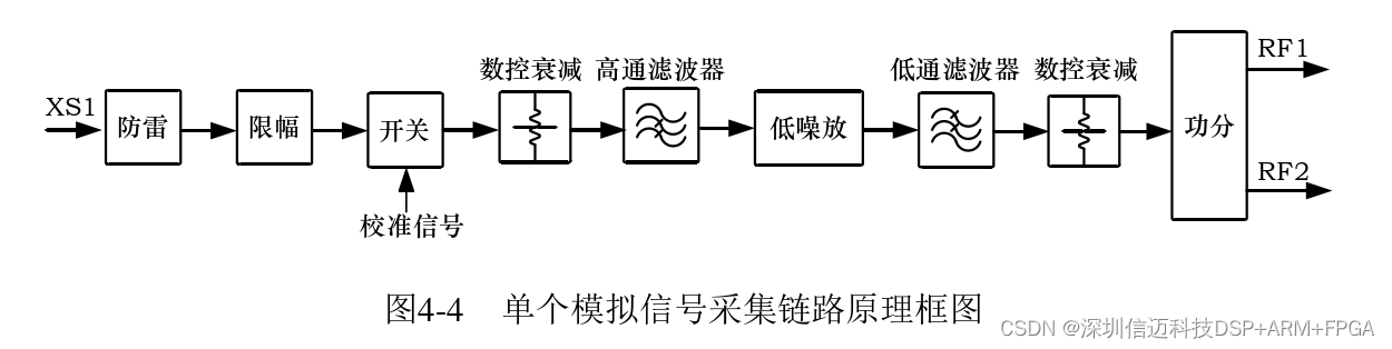
After passing through the lightning protection circuit, the analog signal first goes through a limiter to restrict high-power signal input, and then through a 2-to-1 switch. This switch is primarily used to route the calibration signal to the main signal chain. Subsequently, after spurious suppression and signal amplification by filters and low-noise amplifiers, the signal is output to the digital signal processing circuit. The purpose of the calibration signal is for the ADRV9009 to transmit a calibration signal to correct phase errors in the four receiver links, achieving phase consistency through digital compensation. (1) Gas Discharge Tube The lightning protection circuit is designed using gas discharge tubes. Gas discharge tube protection is added at the input of the analog signal acquisition circuit, providing both lightning strike protection and electrostatic discharge (ESD) protection. This design selects the SG75 discharge tube manufactured by Littelfuse, with specific parameters shown in Table 4-1.
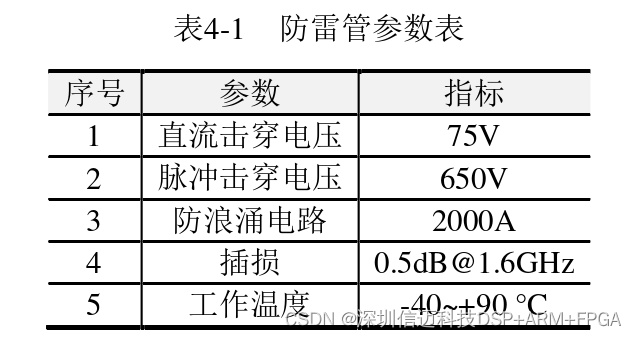
From Table 4-1, it can be seen that the discharge tube can withstand a pulse voltage of 650V and an instantaneous current of 2000A. The insertion loss at 1.6GHz is 0.5dB. (2) Limiter The limiter is used to prevent high-power signals from damaging subsequent chips in the circuit. The selected limiter is the MADL-011021-14150T chip from MACOM, with specific parameters shown in Table 4-2.
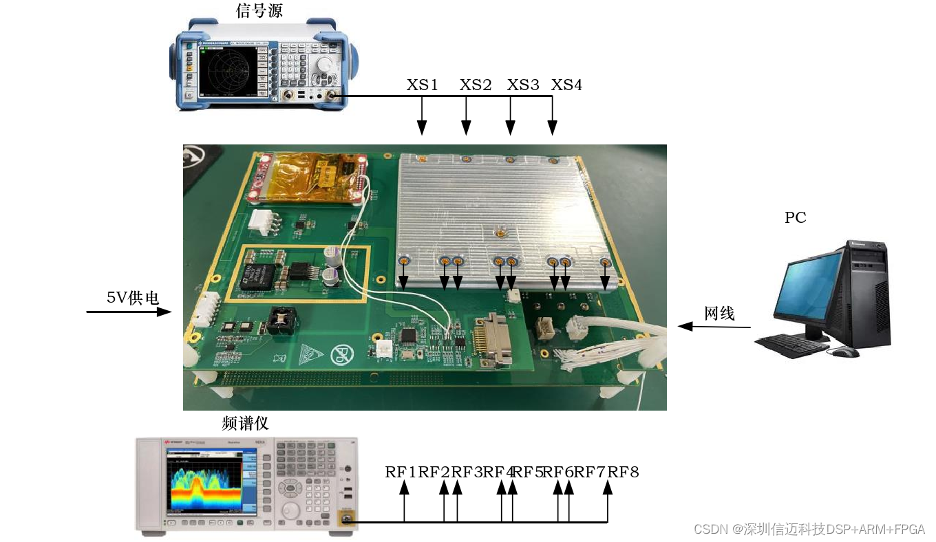
Test Steps
- Power on the circuit board and begin testing when the current is normal. 2) Open the VIVADO software and load the 8MHz bandwidth test bitstream.
- The signal generator outputs a single tone at 1004MHz with -20dBm power, connected to the board's RF1 port via a coaxial cable.
- Configure the ADRV9009 software to set the ADC LO to 1000MHz, capture the RF1 signal, analyze the spectrum, and observe if the target signal is captured.
- Load the 200MHz bandwidth test bitstream, and change the signal generator's single tone to 1100MHz. 6) Configure the ADRV9009 software to set the LO to 1000MHz, capture the RF1 signal, analyze the spectrum, and observe if the target signal is captured.
- Similarly, connect the signal generator to RF2~8 ports, repeat steps 2~6, and test the instantaneous reception bandwidth of the remaining 7 channels.

5.3.2.1 Receiver Sensitivity Test A. Test Principle and Scheme Receiver sensitivity refers to the ability to receive small signals. Receiver sensitivity is related to noise figure, reception bandwidth, and demodulation signal-to-noise ratio (SNR). According to design requirements, when the signal bandwidth is 10MHz and the demodulation SNR is 8dB, the receiver sensitivity should be better than -87dBm. Test scheme: Input a bandwidth signal to the device, and through spectrum analysis, find the minimum signal input power that satisfies an 8dB SNR. B. Test Steps
- After power-on, wait for system initialization to complete.
- Open the VIVADO software and load the 10MHz bandwidth test bitstream.
- The signal generator outputs a 10MHz bandwidth signal at 700MHz with a power of -87dBm. The signal source is connected to the XS1 port via a coaxial cable.
- Configure the ADRV9009 software to set the ADC LO to 700MHz and maximum channel gain. 5) Acquire the signal using VIVADO, analyze the RF1/RF2 spectrum with spectrum software, and observe if the SNR is greater than 8dB. If it is greater than 8dB, decrease the signal generator output power in 0.5dB steps until the SNR is 8dB, then record the signal power at this point. If it is less than 8dB, increase the signal generator input power in 0.5dB steps. Record the signal generator input power when the SNR is greater than 8dB. 6) Change the signal generator input frequency point and similarly test the receiver sensitivity at 1100MHz and 1600MHz. 7) Using the same method, test the linear input level of RF3~8. C. Test Results and Analysis