[Domestically Developed Virtual Instruments] Multi-channel Synchronous Data Acquisition Design Solution Based on ZYNQ7045+V7 FPGA (Part 1)
Multi-channel data acquisition devices are widely used in today's era of information digitalization. Various measured information, such as light, temperature, pressure, humidity, and position, must be sampled and processed by multi-channel signal acquisition systems before they can be further analyzed and utilized by us [37]. In fields with high acquisition rate requirements, such as military, aerospace, aviation, and industrial manufacturing, higher demands are placed on the sampling and processing rates of signal acquisition systems to meet the real-time requirements of signal analysis. The demand for high-speed signal acquisition systems is continuously increasing.
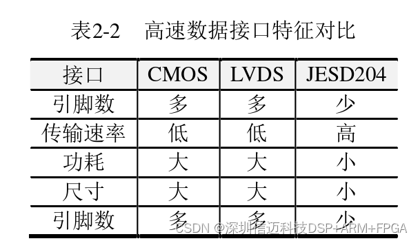
2.2.1.3 JESD204 Interface To address the high-speed transmission limitations of parallel interfaces, JEDEC, the Solid State Technology Association, introduced JESD204, a serial data interface with transmission rates up to 10G. Combining the advantages of differential LVDS current-mode drivers and using CML (Current Mode Logic) structure as its output driver unit, the JESD204 series of standards was launched. By using serial data transmission, it significantly reduces the number of chip pins, simplifies PCB layout, achieves smaller chip sizes, and simultaneously increases data transmission rates. It is particularly suitable for scenarios requiring high conversion speed and high resolution. Table 2-2 compares the typical characteristics of three high-speed data interfaces.
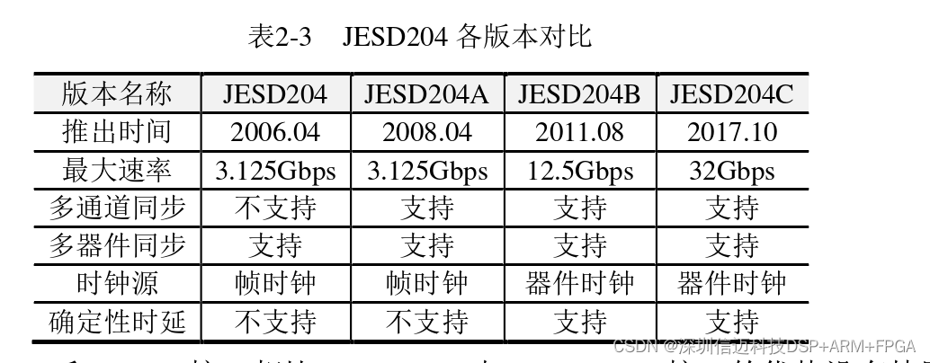
The JESD204 protocol has released a total of 4 versions: JESD204, JESD204A, JESD204B, and JESD204C. In April 2006, JEDEC, the Solid State Technology Association, released the first version of the JESD204 protocol [24]: JESD204. This protocol describes a high-speed serial data link transmission interface between converters and data processors. JESD204 only supports single-lane, single-link data transmission between one converter and a logic device. M-bit data converter chips transmit over a single serial CML lane, with a maximum rate of up to 3.125Gbps [25]. As shown in Figure 2-6.
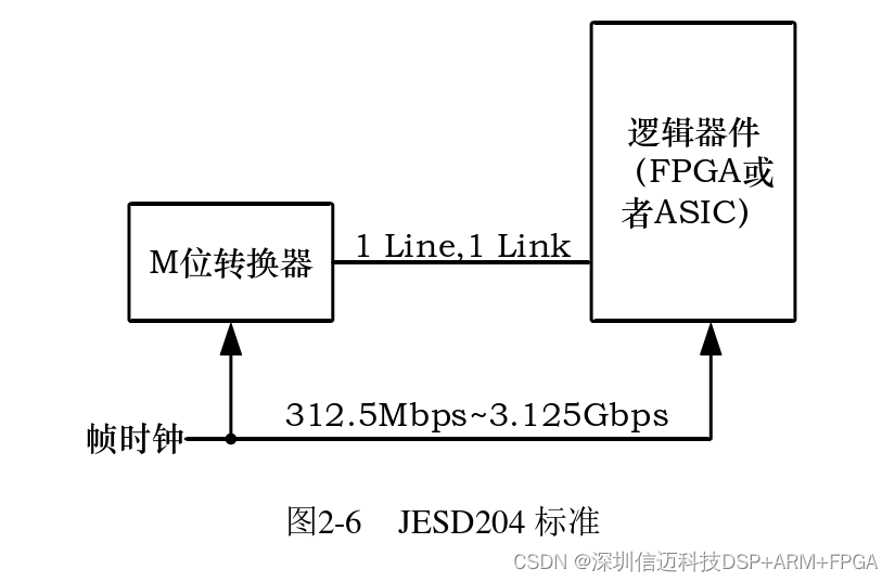
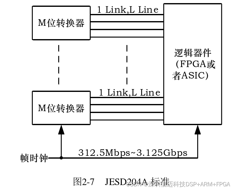
The JESD204 protocol specifies that the data link layer uses 8b/10b encoding, and converters and logic processing devices use the same clock: Frame Clock. By embedding the required clock into the data stream, it avoids the difficulty of aligning data with the clock during high-speed data transmission. In April 2008, JEDEC introduced the JESD204A version. The main added features include:
- A single logic processor can transmit data simultaneously with multiple converter devices.
- Multiple lanes can transmit simultaneously under a single link for a single converter device.
- Data alignment function for multiple lanes under a single link.
In August 2011, JEDEC introduced the JESD204B version. The main changes in this version are:
- Elimination of the frame clock; data converters and logic processors use their respective device clocks, enhancing device usage flexibility.
- Support for deterministic latency, enabling multi-device, multi-channel synchronization.
- Maximum transmission speed increased to 12.5Gbps.
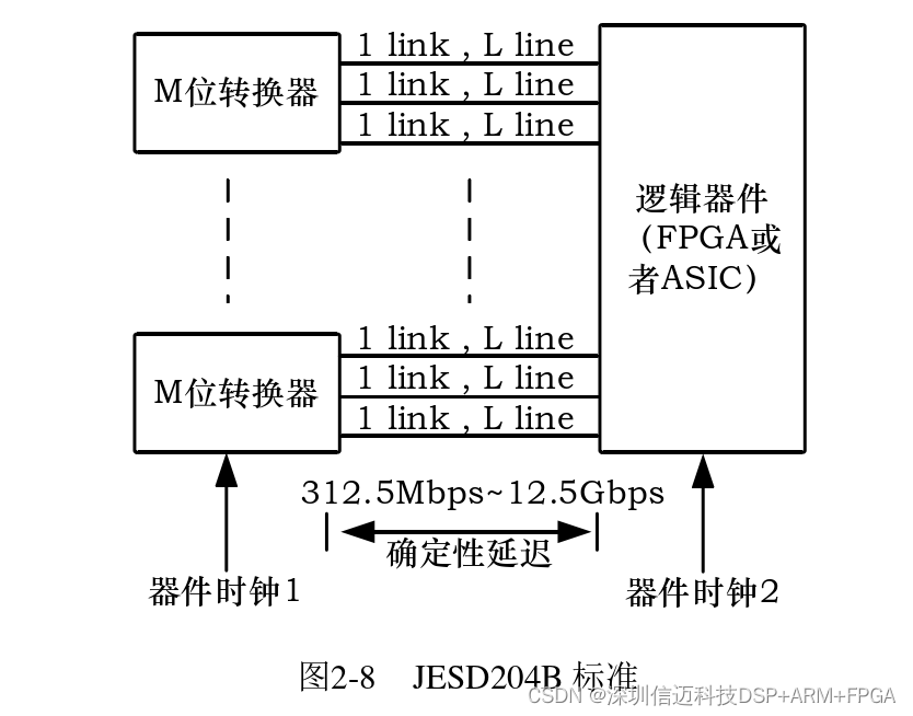
JESD204B has 3 subclasses [26]: Subclass 0, Subclass 1, and Subclass 2. The three subclasses are divided based on their synchronization methods. Subclass 0 is compatible with JESD204A, Subclass 1 uses SYSREF for synchronization, and Subclass 2 uses SYNC for synchronization. Only Subclass 1 and Subclass 2 support deterministic latency, meaning the link latency from data transmission to data reception is fixed. In October 2017, JEDEC released the third revision of the JESD204 standard, JESD204C. The main changes in this version are:
- Maximum lane transmission rate up to 32Gbps.
- For transmission rates from 6.375Gbps to 32Gbps, three subclasses are defined based on link power consumption: C-S, C-M, and C-R.
- Introduction of two encoding schemes: 64B/66B and 64B/80B.

Table 2-3 compares the typical characteristics of the four versions of the JESD204 interface.
Compared to CMOS and LVDS interfaces, the advantages of JESD204 and JESD204A interfaces were not particularly obvious, and they were not widely adopted. However, due to its significant advantages, the JESD204B protocol has been favored by many high-speed converter companies, leading to the introduction of a large number of high-speed converter products based on the JESD204B interface, with typical companies being Analog Devices (ADI) and Texas Instruments (TI). The JESD204C protocol was released later, and user application demand is not yet very strong, so its widespread adoption is currently not as high as that of the JESD204B interface. 2.2.2 Multi-chip Synchronization In multi-channel data acquisition technology, different channels acquire data at the same time, and their phases are identical. However, in practice, due to different physical path delays between channels, multiple raw signals experience varying delays during transmission, resulting in misaligned signal data. Similarly, multiple sampling clocks also have link delays, failing to achieve the effect of synchronous sampling. By calibrating inter-channel delays, and then performing inter-channel delay compensation and correction, the starting points of raw signals from different channels become consistent, and sampling times become synchronized, thereby achieving synchronous data acquisition. Reference [27] proposes a multi-physical quantity collective effect idea, explaining the inter-channel delay time differences caused by multiple physical factors, and achieving data acquisition synchronization through time-base compensation and correction. Multiple physical factors can be divided into analog and digital factors; therefore, multi-channel data acquisition synchronization technology can be categorized into analog signal synchronization and digital signal synchronization. Analog signal synchronization ensures consistent phases for multi-channel analog signals, while digital signal synchronization ensures consistent sampling times for multi-channel digital signals. 2.2.2.1 Analog Signal Synchronization Reference [28] provides a method for multi-chip analog signal synchronization: when multiple analog signal acquisition channels use the same local oscillator (LO), the phase shift effects caused by amplification, filtering, and attenuation in the analog signal reception link can be ignored, thereby achieving analog signal synchronization. Current ADCs generally support single-chip multi-channel analog signal synchronous acquisition, but do not necessarily support multi-chip analog signal synchronization (Multi-Chip Sync, MCS) acquisition. For example, Analog Devices' AD9361 chip, which uses a zero-IF architecture, supports two on-chip channels for synchronization but does not support multi-chip multi-channel analog signal synchronization. If such chips need to achieve multi-chip multi-channel analog signal synchronization, there are two implementation methods:
- One is for multiple ADCs to share a single local oscillator.
- The other is to measure the phase difference of multiple internal LOs and then calibrate it using an FPGA algorithm. Method one requires extremely high quality for the local oscillator signal. Regarding method two, reference [29] provides a method for achieving multi-chip AD9361 phase synchronization through algorithmic compensation. 2.2.2.2 Digital Signal Synchronization In common multi-channel signal synchronous acquisition methods, a single clock is used, and data from multiple ADC chips is acquired after slight adjustments based on link delays. During acquisition, the synchronization clock of one ADC is selected as the sampling clock. This clock shares the same source as the data from each ADC, but their phase relationship is unknown [30]. By using the input/output delay unit function within the FPGA, the data signals input from each ADC are delay-adjusted to correct the phase difference between the data signal and the sampling clock, ensuring that the sampling clock can correctly capture the corresponding data. This achieves multi-chip digital synchronous sampling, which is simple in structure and easy to implement in engineering. Taking Analog Devices' ADRV9009 chip [31] as an example, this chip supports the JESD204B interface. By synchronously coordinating and managing the configuration of two FPGAs on the board, it is possible to configure multiple ADRV9009 chips across these two FPGAs, thereby meeting the requirements for multi-chip ADRV9009 synchronous acquisition. The synchronization network for multiple ADRV9009 chips in this device is shown in Figure 2-10.
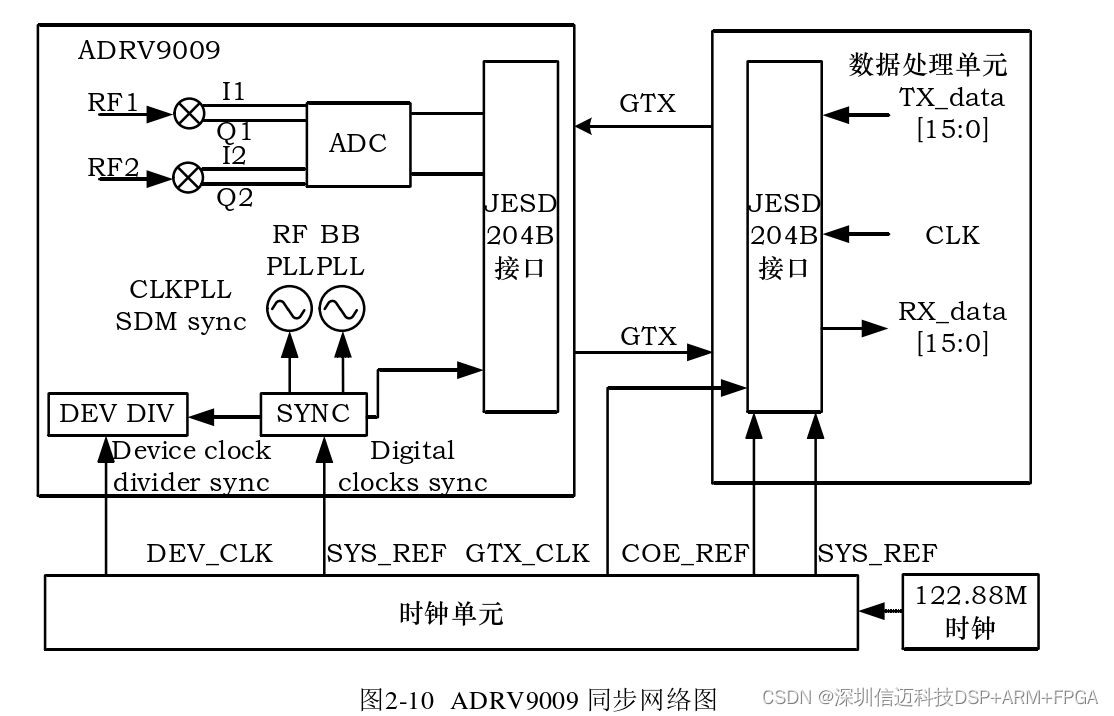
The JESD204B interface can achieve multi-chip synchronization using its built-in synchronization protocol under a common clock source. From the ADRV9009 synchronization network diagram, it can be seen that this analog integrated chip contains not only the JESD204B interface but also an internal Baseband Phase-Locked Loop (BBPLL), Radio Frequency Phase-Locked Loop (RFPLL), input divider module (DEVDIV), and synchronization management module (SYNC). After the reference clock enters the chip, it also passes through the internal synchronization management module, divider module, and baseband PLL before being distributed for JESD204B use. Therefore, to achieve multi-chip synchronization, synchronous triggering of each internal module of the ADRV9009 chip is also required. 2.2.3 Multi-thread Synchronization Since multiple data converters require synchronous acquisition, individual data collectors cannot be configured sequentially. To meet the demand for simultaneous configuration, the multi-tasking feature of the operating system is utilized, meaning multiple threads are created within a single application to complete the parameter configuration tasks for each data collector separately. Taking Analog Devices' ADRV9009 chip as an example, the core to achieving multi-chip ADRV9009 synchronization is the requirement for three SYSREF pulse signals with identical phases. Each thread, when configuring the ADRV9009, will block while waiting for three SYSREF pulse signals. When the main thread detects that each ADRV9009 is in a pulse-waiting state, it controls the clock management chip to generate three SYSREF pulses, thus ensuring that multiple ADRV9009 chips simultaneously receive three in-phase SYSREF pulses.