STM32 ARM+FPGA-based Power Quality Analyzer Solution (Part 1) Hardware Design
This chapter primarily presents the design goals and hardware design scheme of this system. It then details the hardware circuit design process, including the data acquisition board and the FPGA+ARM control board.
3.1 System Design Goals
The main objective of this system is to achieve high-precision measurement and data analysis of power quality indicators. The specific technical specifications are as follows:
-
Power Quality Indicator Measurement Accuracy: (1) Voltage: ±0.3% of rated voltage; (2) Current: ±0.5%; (3) Frequency: ±0.01 Hz; (4) Three-phase unbalance: ±0.2%; (5) Harmonic analysis: 1st-17th.
-
Capable of real-time display of power quality indicators and three-phase voltage and current waveforms, enabling data sharing and good human-machine interaction.
-
Capable of storing grid operation data.
3.2 System Overall Scheme
Control circuit structures in measurement systems vary widely, including control circuits with standalone FPGA, ARM, or DSP chips, as well as multi-architecture control circuits based on FPGA+ARM, DSP+FPGA, DSP+ARM+FPGA, etc. This design adopts an FPGA+ARM dual-processor mode as the control circuit. FPGAs have a large number of I/O ports, fast data reception and processing speeds, strong capability for capturing the shortest narrow pulses, and high anti-interference ability, ensuring the accuracy and continuity of the data acquisition process. FPGAs also feature hardware multipliers and parallel data processing, providing assurance for the extensive multiply-accumulate operations involved in subsequent FFT algorithms. ARM is a commonly used processor, characterized by high performance, low power consumption, numerous integrated library functions for convenient development, and a wide array of peripherals, providing ample room for future system function expansion. The system hardware block diagram is shown in Figure 3.1.
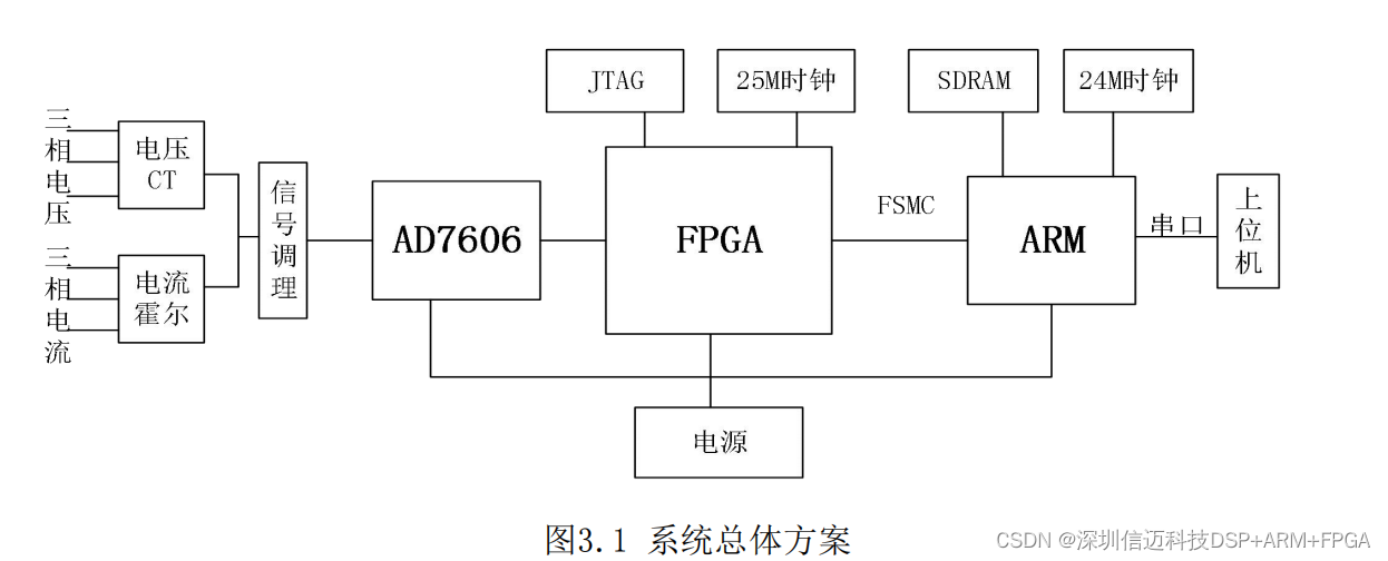
As shown in the figure above, the hardware circuit mainly includes the data acquisition section, the FPGA+ARM control section, and the host computer section.
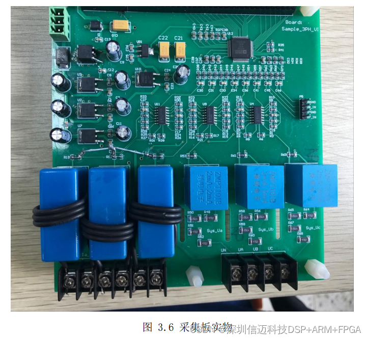
The design of the data acquisition board includes the power supply circuit, front-end voltage and current transformer circuits, voltage follower circuits, and an AD7606-based analog-to-digital conversion circuit. The FPGA+ARM control section mainly includes power supply circuits for FPGA and ARM, download circuits, serial port circuits, clock circuits, etc. The host computer display module is host computer software written in C#. The specific working process of the system is as follows: First, the three-phase high voltage and current signals from the power grid are adjusted to the A/D input range via voltage and current transformers and voltage follower circuits composed of operational amplifiers. Then, the FPGA controls the analog-to-digital converter to achieve high-speed synchronous sampling of 6-channel signals. Within the FPGA, the design of the three-phase phase-locked loop and FFT calculation module is completed, and historical data is stored using SDRAM. FPGA and ARM communicate via FSMC. The embedded real-time operating system FreeRTOS is ported to the ARM processor to handle thread tasks such as data reading and writing between FPGA and ARM, serial communication between ARM and the host computer, and calculating various power quality parameters after floating-point operations. Finally, various power quality indicators are displayed and analyzed in real-time through the host computer software.
3.3 Data Acquisition Module
3.3.1 Sampling Process
Data acquisition, as the front-end circuit of the system, directly affects the measurement accuracy of electrical parameters and real-time display speed. In recent years, digital sampling has been widely applied in the field of electrical measurement. Signal acquisition is divided into two types: DC sampling and AC sampling:
(1) DC sampling involves reducing the amplitude of AC voltage or current signals using transformers or current/voltage transformers, then converting them into DC signals via a rectifier circuit for acquisition. Its main drawbacks include: a large time constant of the R-C filter circuit, affecting real-time performance; significant errors when measuring signals containing harmonics or noise; and complex transmitter equipment that is difficult to maintain later.
(2) The basic principle of AC sampling [33] is to use voltage and current transformers to isolate, filter, phase shift, and amplify the measured AC voltage and current signals. A microprocessor then samples their continuous instantaneous values to obtain discrete time-domain sampling sequences. Subsequently, algorithms are applied to numerically process the sampled value sequences to calculate the measured quantities. AC sampling eliminates complex rectifier circuits, requiring only simple filtering and amplitude amplification/attenuation conditioning circuits. Because AC sampling targets the instantaneous values of signals, it offers good real-time performance and minimal phase distortion. With the rapid development of electronic technology in recent years, DSPs and high-speed A/D converter chips have provided hardware support for AC sampling. AC sampling is gradually replacing DC sampling and becoming the mainstream sampling method in electrical measurement.
3.3.2 AD7606 Analog-to-Digital Conversion Circuit
The AD converter is the core of the entire acquisition board, and the quality of its performance indicators, such as conversion speed and resolution, directly affects the final measurement results [34]. There is a wide variety of AD converters on the market, with performance varying greatly between different companies and product series. For high-precision data acquisition, a high-precision analog-to-digital converter is indispensable.
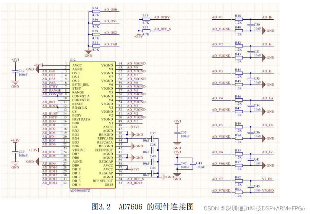
Based on design requirements such as channel count, sampling rate, and synchronous sampling, this design selects Analog Devices (ADI)'s 8-channel, 16-bit AD7606 synchronous sampling chip. It is one of the commonly used sampling chips in power line measurement systems. It features a sampling rate of up to 200 kSPS, supports ±5 V and ±10 V bipolar signal inputs, is powered by a single 5 V analog supply, integrates a 2.5 V reference voltage source, and provides oversampling and digital filtering functions. The digital output mode can be set to parallel or serial output as needed. Traditional successive approximation register (SAR) ADCs require an operational amplifier at the input front-end to drive the internal sampling capacitor for sampling. However, the AD7606 integrates a low-noise, high-input impedance signal conditioning circuit with an input buffer featuring a 1 MΩ analog input impedance. Therefore, the AD7606 does not require external driving or filtering circuits, greatly simplifying the front-end design. The hardware connection diagram for the AD7606 is shown in Figure 3.2.
3.4 FPGA+ARM Control Module
3.4.1 FPGA Selection
FPGA (Field-Programmable Gate Array) evolved from programmable devices such as PAL, GAL, and CPLD. It is a type of semi-custom circuit within Application-Specific Integrated Circuits (ASICs) [36], featuring static re-programmable functionality. Users can reconfigure internal logic modules and I/O ports through software programming to change hardware functions. This overcomes the inflexibility of custom circuits, significantly improves integration, and its unique parallel processing greatly enhances data computation speed. In recent years, microprocessors have developed rapidly, with increasing integration. A digital circuit can be formed using just an FPGA chip along with its power supply, configuration, and clock circuits, greatly reducing peripheral circuitry. Due to the rich programmable resources, parallel data processing, and strong flexibility of FPGA processors, they are widely used in real