[Domestic Virtual Instrument] Zynq-Based Radar 10Gbps High-Speed PCIe Data Acquisition Card Solution (Part 3) Software Design
4.1 Introduction
This chapter presents the system software design based on the analysis conclusions from Chapter 2. The software design encompasses logic design, embedded software design, and host PC software design. In the logic design, the ADC module, Aurora module, DDR3 SDRAM module, and PCIe module are analyzed and designed. Based on the IP cores provided by Vivado, the logic code for each module is implemented, and data interfacing issues among modules are resolved. The embedded design involves system and kernel porting, enabling system boot-up through the PS core of Zynq. For the host PC software design, driver development tools are first introduced, followed by an overview of the overall host software architecture.
4.2 Logic Software Design
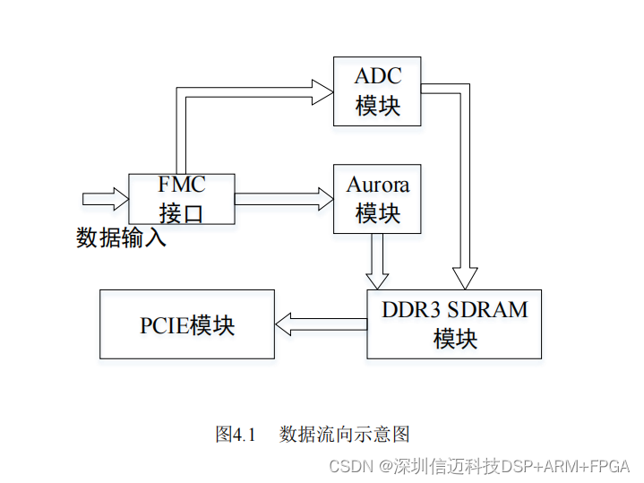
Since the data on the FMC interface of the carrier card depends on the type of mezzanine card connected, either the ADC module or the Aurora module is selected accordingly. When an AD mezzanine card is connected, the ADC module is enabled; when an optical fiber mezzanine card is connected, the Aurora module is enabled. The corresponding module data is first buffered in DDR3 SDRAM before being transmitted to the PC via the PCIe interface. The data flow is illustrated in Figure 4.1.
The ADC module serves as the driver for the AD mezzanine card, supporting a sampling rate of 1 Gsa/s with a data resolution of 12 bits. The Aurora module acts as the driver for the optical fiber mezzanine card, implementing the Aurora protocol with 4 lanes, each operating at 10 Gbps, resulting in a total data rate of 40 Gbps. The PCIe interface uses PCIe 2.0 protocol in x8 mode, with a per-lane rate of 5.0 Gbps, achieving a total bandwidth of 40 Gbps. The DDR3 SDRAM module buffers data from either the Aurora or ADC modules. Vivado provides IP cores for Aurora, PCIe, and MIG, offering interface solutions for the Aurora protocol, PCIe protocol, and DDR3 SDRAM, respectively. Each module is detailed below.
4.2.2 ADC Module Logic Design
The ADC chip on the AD mezzanine card supports a maximum sampling rate of 1.6 Gsa/s. According to the performance analysis in Chapter 2, the ADC sampling rate must be no less than 706.6 Msa/s. In this design, the ADC sampling rate is set to 1 Gsa/s.
The ADC chip operates in dual-edge sampling mode, allowing the sampling rate to be twice the sampling clock frequency. A 500 MHz differential clock signal is required. A 500 MHz single-ended clock can be generated using the MMCM resources within the Zynq chip, then converted to a differential clock using Xilinx's OBUFDS primitive.
Since the ADC operates in dual-edge sampling mode, the DES pin of the ADC chip must be pulled high. The signal coupling method is AC coupling, requiring the VCMO pin to be set low. In dual-edge mode, the ADC chip supports multiplexed mode, which allows data line multiplexing. The timing diagram for multiplexed mode is shown in Figure 4.2 [25].
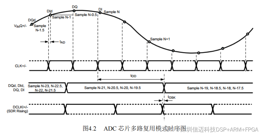
In the figure, CLK+/- is the sampling clock signal, DQd, Did, DQ, and DI are the ADC data lines, and DCLKI+/- is the data synchronization output clock for channel I. As shown, in dual-edge and multiplexed mode, after four conversions, data is sequentially output to DQd, Did, DQ, and DI. Simultaneously, a clock signal at half the conversion rate (250 MHz in this case) is output on DCLK+/-.
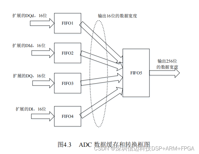
The data width is 12 bits, but the FIFO width in the DDR3 SDRAM module is 256 bits, which is not an integer multiple of 12. To resolve this, each 12-bit data channel is extended to 16 bits and stored in smaller FIFOs. These are then aggregated into a single FIFO that outputs data at 256-bit width. The data buffering architecture is shown in Figure 4.3. FIFO1–FIFO4 are synchronous FIFOs with read/write widths of 16 bits, clocked by the DCLK+/- signal from the ADC chip (converted from differential to single-ended). The outputs of these four FIFOs are written into FIFO5, an asynchronous FIFO with a 64-bit write width and 256-bit read width, which can be directly interfaced with the DDR3 SDRAM module.
4.2.3 Aurora Protocol Logic Design
The optical interface uses the Aurora protocol with 4 lanes, each operating at 10 Gbps, achieving a total data rate of 40 Gbps. Data transmission over the optical interface is implemented using the Aurora IP core provided by Vivado, which supports two encoding schemes: 8B/10B and 64B/66B. This design adopts 64B/66B encoding to improve bandwidth efficiency. The core instantiation process is shown in Figure 4.4.
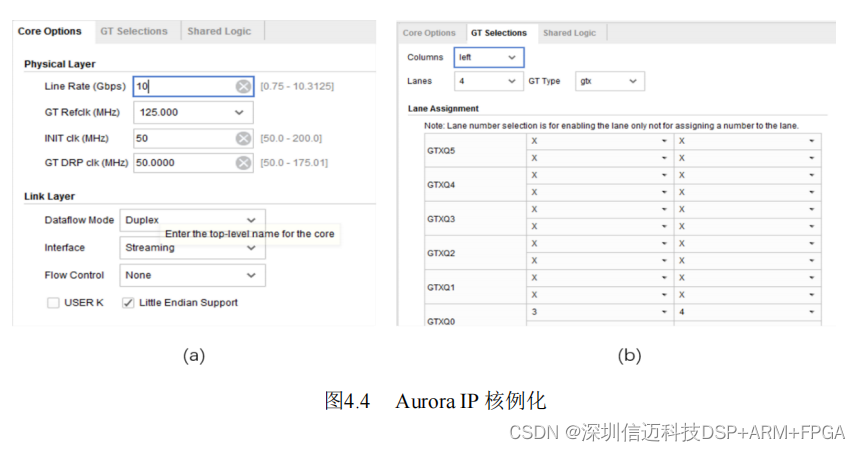
During core instantiation, the transmission rate is first specified as 10 Gbps. Based on the hardware design, the reference clock is set to 125 MHz. Full-duplex streaming mode is selected for ease of design and use. Then, the channel mapping on the FPGA is defined.
The instantiated core is shown in Figure 4.5.
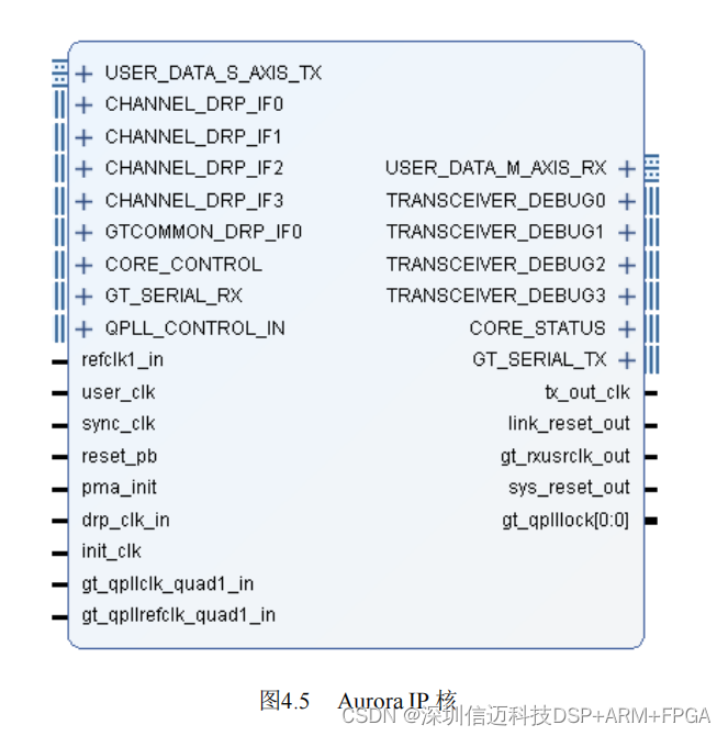
The Aurora IP core uses the AXI bus protocol for data transmission and reception, with timing compliant with the AXI protocol and a data width of 256 bits. The DRP (Dynamic Reconfiguration Port) is used to configure channel rates and parameters. The DEBUG signals include channel status and eye diagram testing, useful for debugging.
The AXI interface signals and their functions of the Aurora IP core are listed in Table 4.1.
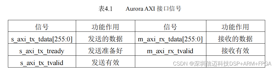
The Aurora encoding scheme is 64B/66B, with a per-lane data width of 64 bits. Thus, the total data width across four lanes is 256 bits. The transmission uses streaming mode, which does not require frame end or valid byte indicators, so the AXI interface lacks _tkeep and _tlast signals.
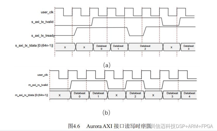
The AXI transmit and receive timing diagrams for the Aurora IP core are shown in Figure 4.6 [26], where (a) shows the transmit timing and (b) the receive timing, with n representing the number of channels (n=4 in this case).
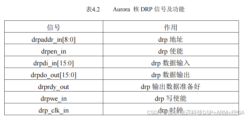
In practical applications, the Aurora transmission rate and parameters are typically fixed, so DRP configuration is usually unnecessary. The IP core includes four DRP ports, one for each Aurora channel. Taking channel 1 as an example, the DRP port signals and their configurations are shown in Table 4.2.
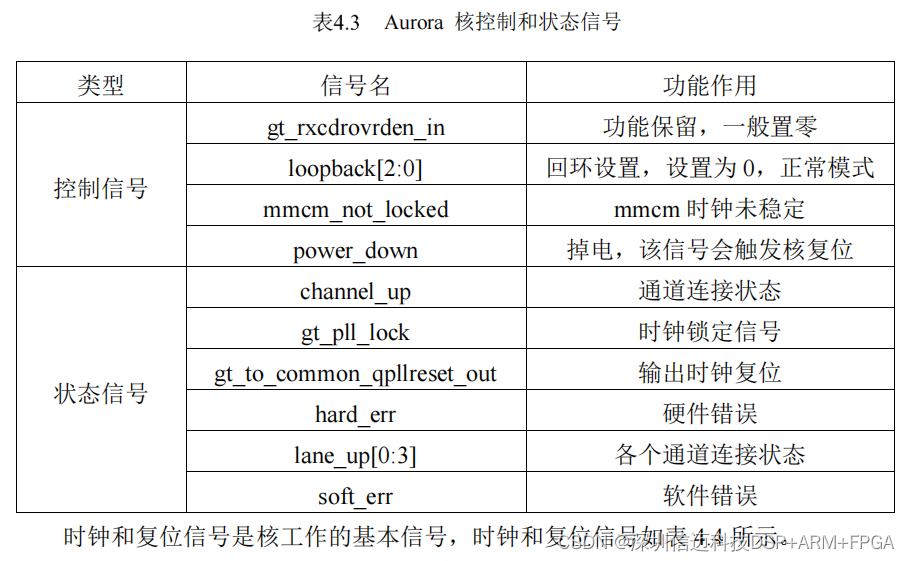
The Aurora core includes control and status signals. Control signals manage functions such as loopback and power-down, while status signals indicate channel link status, reset conditions, and hardware/software errors. The functions of these control and status signals are detailed in Table 4.3.
The Aurora design also uses FIFOs as interfaces between modules. Since the AXI interface has a 256-bit data width, the FIFO is designed with the same width. Data flows from an upstream FIFO into the Aurora core, then through a downstream FIFO to subsequent modules.
4.2.4 DDR3 SDRAM Logic Design
DDR3 SDRAM is typically used for data buffering. The basic principle involves reading and writing data to a specific address range within the DDR3 SDRAM. A common example is in PCs, where each application occupies a specific address range in memory, meaning DDR3 SDRAM addresses are managed in blocks.
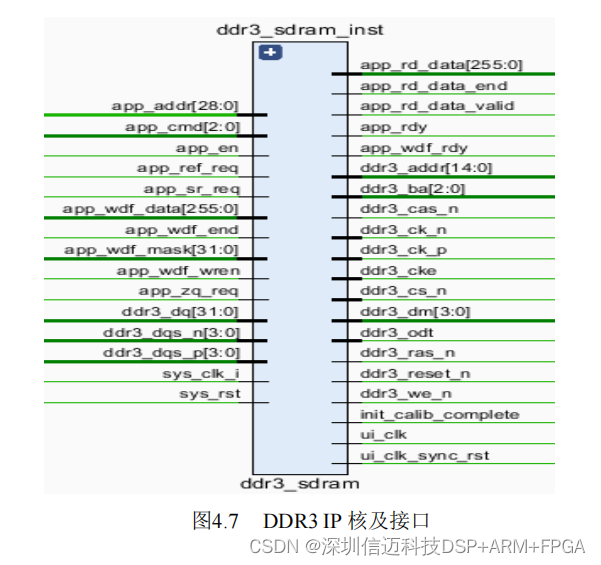
In this design, to meet the data buffering requirements of the radar emitter signal identification platform, the entire address space of the DDR3 SDRAM is used for data storage, fully utilizing its capacity to implement a large-capacity FIFO. Vivado provides the MIG (Memory Interface Generator) core specifically for DDR3 SDRAM interfacing, which, along with peripheral logic, enables read and write operations. The acquisition card uses two DDR3 SDRAM chips, each with a 32-bit data width and a 15-bit address width.
During MIG core instantiation, the DDR3 operating clock and output clock ratio are first set—here to 600 MHz. With a 32-bit data width, the theoretical read/write rate is 38.4 Gbps. However, in practice, DDR3 SDRAM refresh operations reduce the effective rate below the theoretical maximum. Next, impedance and address configurations are set. Impedance settings ensure impedance matching for reliable and stable signal transmission. Two address mapping options are available: ROW+BANK+COLUMN or BANK+ROW+COLUMN. The BANK is determined by the bank pins of the DDR3 chip, while ROW and COLUMN refer to the memory matrix's rows and columns, defined by the chip's characteristics. Finally, physical pins are assigned to the DDR3, completing the core instantiation.
The instantiated MIG IP core and its interface are shown in Figure 4.7: