Implementation Solution for a Large-Capacity Solid-State Storage Board Based on NXP + FPGA
1 Overview
In recent years, large-capacity data storage devices have primarily relied on stacked combinations of mechanical hard drives due to limitations in software and hardware development. Mechanical hard drives use platters as the storage medium and mechanical motors, suffering from drawbacks such as low vibration resistance, poor low-temperature performance, and high noise. Solid-state drives (SSDs), on the other hand, use semiconductors as both the storage medium and control carrier. Lacking mechanical components, they offer advantages such as shock resistance, wide operating temperature range, noiseless operation, high reliability, and energy efficiency, playing an increasingly significant role in large and complex electronic equipment. Large-capacity solid-state storage technology is attracting widespread attention.
This article, in response to the needs of a specific project, adopts an implementation method where an ARM processor and a Field-Programmable Gate Array (FPGA) control and manage a solid-state storage board, to achieve a single-board (6U CPCI standard card) solid-state storage capacity of no less than 4TB.
2 System Architecture
For different applications, with ARM as the processor, FPGAs can be extended to implement storage control boards of various capacities, and the basic system architectures are similar. This article will illustrate a 6U CPCI standard card implemented by our company using a dual-FPGA control technology, supporting a maximum single-board storage capacity of 4TB.
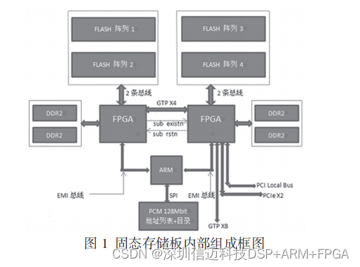
The solid-state storage board consists of 128 NAND FLASH chips (32 GB each), with every 32 NAND FLASH chips forming a group, resulting in a total storage capacity of 4 TB. It uses 2 high-performance FPGAs and 1 ARM processor for logical control of the NAND FLASH, with a total of 4 64-bit FLASH buses. Each group of 32 NAND FLASH chips is driven by one FLASH bus, achieving read/write speeds of up to 260 MB/s, and the single board can reach a total bandwidth of 1040 MB/s. By selecting the GTP×4 high-speed serial bus, it can meet the project requirement for a storage speed of 448 MByte/s. The internal block diagram of the solid-state storage board is shown in Figure 1.
3 ARM Processor, FPGA Selection, and Driver Algorithm Implementation
NXP Semiconductors implements the LPC2478 microcontroller with a 16- or 32-bit ARM7TDMI-S CPU core, which comes with real-time embedded trace and JTAG debug interfaces. The LPC2478 microcontroller operates at frequencies up to 72 MHz and has 512 KB of Flash program memory, enabling In-Application Programming (IAP) and In-System Programming (ISP) functionalities. The LPC2478 can execute both 16-bit Thumb instructions and 32-bit ARM instructions, allowing engineers to selectively optimize applications at the program level. Its 98 KB on-chip SRAM can store data powered by the RTC, and for high-performance CPUs, it can be accessed via the ARM local bus. Through a dual AHB bus system, the execution of on-chip Flash programs and synchronous Ethernet USB DMA, as well as other DMA operations, are guaranteed not to preempt each other. The LPC2478 microcontroller is also highly suitable for various communication applications, possessing a rich set of serial interfaces and other peripherals.
The Virtex-5 series, as the second-generation Advanced Silicon Modular Block (ASMBLTM) column-based architecture, features five distinct sub-families (LX, LXT, SXT, TXT, and FXT), making it the most diverse series among FPGAs. Key applications include high-performance logic with advanced serial connectivity, high-performance systems with dual-density advanced serial connectivity, high-performance signal processing applications with advanced serial connectivity, high-performance embedded systems with advanced serial connectivity, and high-performance general-purpose logic applications. Each platform offers unique features to meet the demands of various advanced logic designs. In addition to the most advanced high-performance logic structures, Virtex-5 FPGAs integrate a large number of IP hard-core system-level modules, supporting up to 330,000 logic cells and up to 17 external analog input channels, featuring multi-rate FIFO support logic, and allowing access to system monitors via JTAG TAP or internal structures.
The Virtex-5 FPGA chip used in this solid-state storage board also features FLASH controller functionality, integrating multiple technologies into the overall FLASH control, such as wear-leveling management, real-time bad block elimination, and error correction, thereby ensuring the correctness, stability, and security of stored data. These FLASH control technologies have been stably applied in multiple projects. The front view of the physical product is shown in Figure 2.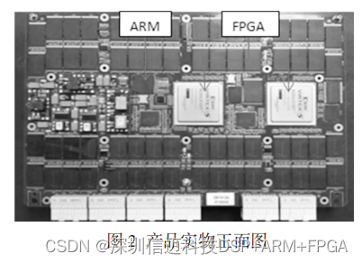
Among these, wear-leveling management technology employs a sequential cyclic management algorithm, which includes linear lists (sequential lists and linked lists), and based on how data recording devices access data for read/write operations, it evenly distributes ERASE and PROGRAM operations across all blocks in the storage space, thereby ensuring the overall lifespan of the hardware.
Real-time bad block elimination technology uses a bad block real-time monitoring circuit method, which monitors the status of FLASH blocks in real-time during read/write operations to identify, mark, and replace BAD BLOCKs across the entire storage space, effectively ensuring real-time elimination of bad blocks.
Error correction technology employs the BCH algorithm for binary channels, characterized by strong error correction capabilities, simple construction, and easier encoding compared to other codes. Furthermore, it utilizes a hardware high-speed circuit parallel operation mode, thereby achieving high-performance BCH encoding and decoding algorithms, ensuring the correctness of FLASH data.
Although large-capacity NAND Flash memory offers many advantages, it is susceptible to the random generation of unavoidable bad blocks. If this bad block issue is not properly addressed, it will lead to a higher failure rate. When hardware failures occur in FLASH chips, the product must still meet the actual data storage requirements for urgent and temporary reconnaissance missions in terms of storage speed or capacity. This necessitates further improvement in the storage board's fault tolerance, allowing the product to continue operation through derated usage in the event of hardware failure. The derating design includes two functions: automatic hardware fault detection and derating processing. The principle block diagram of derating processing during hardware failure is shown in Figure 3.
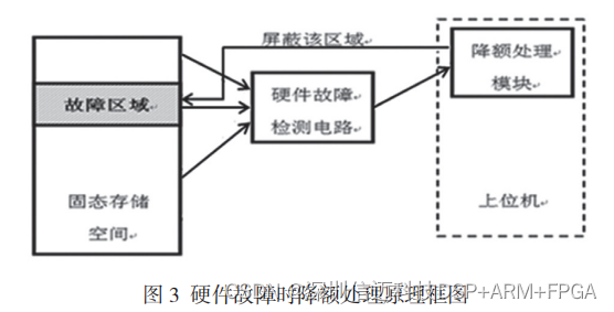
Upon product power-on, the automatic hardware fault detection function performs a hardware status check on all NAND FLASH chips on the storage board. If a hardware fault is detected, it reports the faulty area to the upper layer.
To ensure the storage board can still operate normally when a fault occurs, the upper-layer derating processing function, upon receiving a hardware fault report, can effectively mask the faulty area and handle the hardware fault.
4 Development Tool Usage and Debugging Process for Implementation
-
ARM Debugging: In this example, the microcontroller development environment used with the NXP (LPC2478FET208) microprocessor is Keil uVision4. For debugged programs, an ARM download emulator can be used to verify correct downloading and confirm that the program loads and runs normally. If abnormal phenomena occur, corresponding troubleshooting and subsequent low-level formatting can be performed.
-
FPGA Debugging: This example uses Xilinx ISE Design Suite 13.3 as the development environment. Through an emulator, the hardware FPGA program can be compiled, debugged, and downloaded, including scanning the soldering status of the FLASH array. If abnormal conditions are found on the FLASH read ID or STATUS signal lines, the specific location of the FLASH error can be determined by the FLASH's IO values and chip select signals. Figure 5 shows the use of the ChipScope Pro Analyzer tool to scan the FLASH status to rule out poor soldering and FLASH chips with bad sectors.
Similarly, after the preliminary debugging work is completed, simulated tests are performed using internal signal sources for recording and playback. This allows for verifying the correctness of data storage and retrieval for the entire solid-state storage board.