[Domestic Virtual Instrument] High-Precision 32-Bit Data Acquisition Solution Based on DSP+FPGA+ADS1282 (Part 3): System Performance Testing
System Performance Analysis and Testing
This chapter first analyzes the circuit noise and temperature drift of the system, then conducts performance testing on the data acquisition system and performs analysis on the test data.
5.1 Noise and Temperature Drift Analysis of High-Precision AD Conversion Circuit
5.1.1 Resistor Noise and Temperature Drift
1. Resistor Noise
Resistors are a source of noise, the severity of which depends on resistance value, temperature, applied voltage, and resistor type. Proper selection of resistors is one of the most effective methods to avoid or reduce noise or distortion in signal paths.
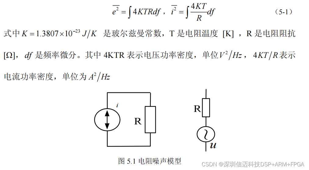
Thermal noise in resistors arises from the random motion of electrons within the conductor. The overall noise of a resistor consists of multiple components, with thermal noise being the most typical. A notable characteristic of thermal noise is that it is independent of resistor material—under the same resistance and temperature conditions, the thermal noise of any resistor type is identical. Figure 5.1 shows the noise model of a resistor in a circuit, which can be equivalently represented as a noiseless resistor in parallel with a current noise source, or as a noiseless resistor in series with a voltage noise source. The root mean square (RMS) of the voltage or current noise source can be expressed as:
Noise index (NI) is defined as the RMS noise voltage (in μV) generated per 1 V DC voltage drop across the resistor over a decade bandwidth, typically expressed in dB. It serves as a metric for comparing noise levels of resistors made from different materials. As shown in Figure 5.2, wirewound and metal film resistors have relatively low noise indices [42]. Carbon-based resistors (e.g., carbon composition and carbon film resistors) exhibit higher current noise. Metal film resistors have lower noise, while wirewound resistors have the lowest noise, though they are physically larger. After comprehensive analysis, high-precision metal film resistors are used in the op-amp sections of this design, while high-precision metal foil resistors are selected for current sensing.
2. Resistor Temperature Drift
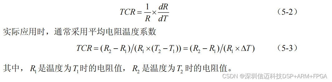
Generally, resistor values are not constant and undergo slight changes with temperature. The temperature coefficient of resistance (TCR) represents the ratio of the increase in resistance per 1°C rise in temperature to the original resistance, expressed in ppm/°C. It can be represented as:
5.1.2 Op-Amp Noise and Temperature Drift
1. Op-Amp Noise
Noise sources in operational amplifier (op-amp) circuits generally include shot noise, thermal noise, flicker noise (1/f noise), burst noise, and avalanche noise [43].
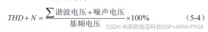
Internal op-amp noise is typically reflected in parameters such as total harmonic distortion (THD), THD plus noise (THD+N), and equivalent input noise voltage. THD refers to the ratio of the RMS voltage of harmonic components of the fundamental frequency in the output signal to the total RMS voltage of the output signal. THD+N is the ratio of the sum of the RMS voltage of the noise and harmonic components to the RMS voltage of the fundamental frequency component [44]. THD+N can be expressed as:
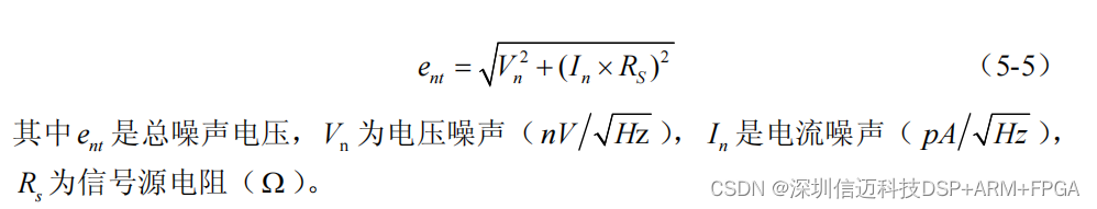
The equivalent input noise voltage parameter represents internal noise voltage referred to a voltage source in series with the non-inverting input. This parameter is frequency-dependent and expressed in V/√Hz. For designers, the noise generated by a device in a circuit can be calculated using formula (5-5):
2. Op-Amp Temperature Drift
The temperature drift of the entire amplification circuit depends on discrete components connected around the op-amp, primarily the temperature drift of resistors and the op-amp's own temperature drift. The op-amp's intrinsic temperature drift is mainly reflected in the temperature drift of the input offset voltage. Input offset voltage, denoted as V_OS, is the voltage that must be applied between the two input terminals to nullify the internal DC voltage mismatch of the op-amp. It compensates for unavoidable mismatches caused by process variations. The input offset voltage varies with temperature, and this variation is characterized by the temperature coefficient of input offset voltage, α_VIO, defined as the ratio of the change in input offset voltage to the change in chip temperature.
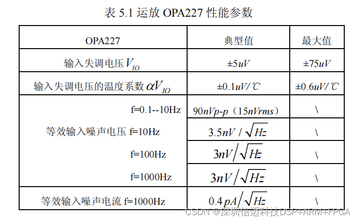
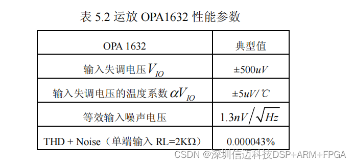
The analog section of this system uses two types of operational amplifiers, with performance parameters listed in Tables 5.1 and 5.2.
5.1.3 Estimation of Total Noise and Temperature Drift in Analog Front-End Signal Processing Circuit
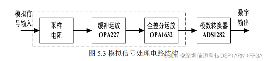
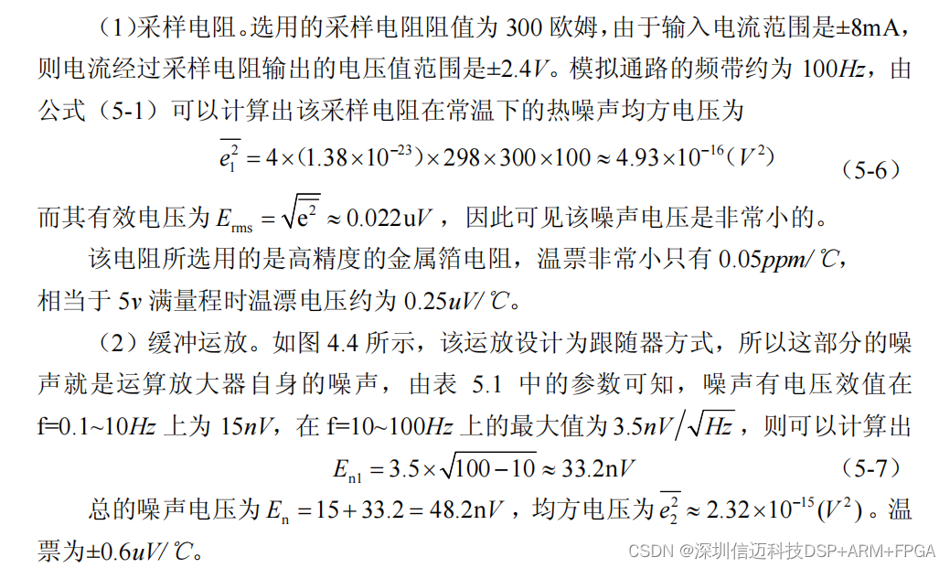
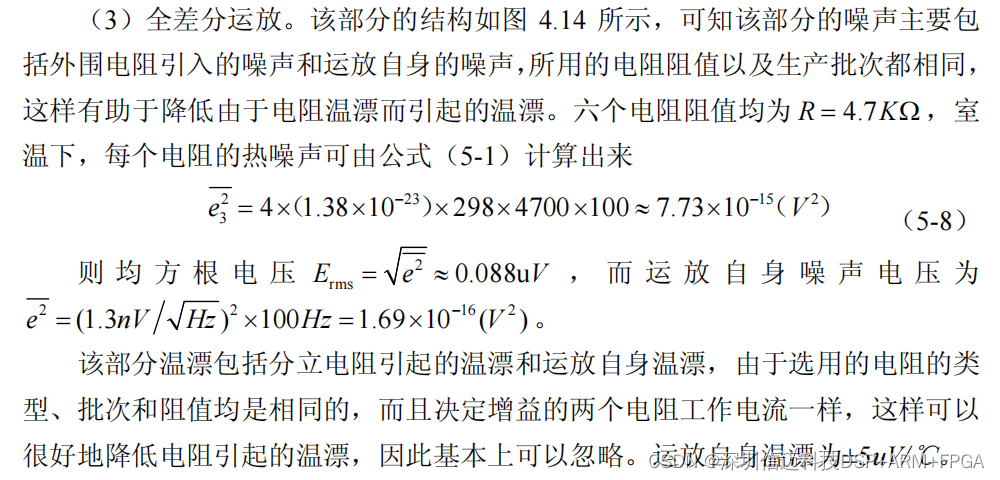
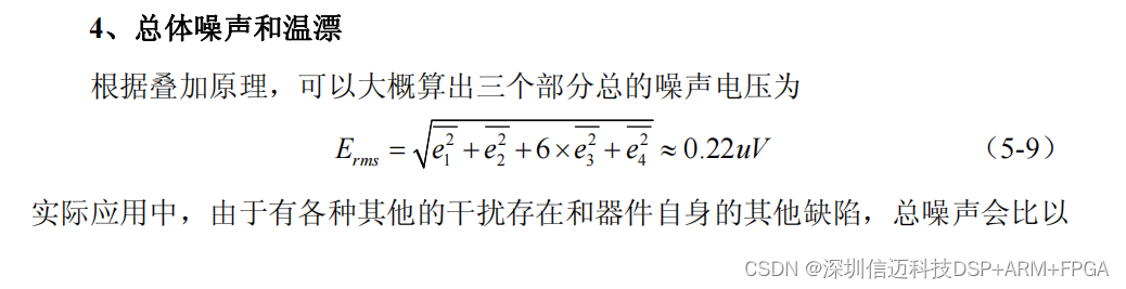
The structure of the analog front-end signal processing circuit is shown in Figure 5.3. It includes a current-sense resistor, buffer op-amp, and signal conditioning op-amp (OPA1632 fully differential amplifier), with a designed bandwidth of 0–100 Hz.
5.2 Data Acquisition Test Methods
5.2.1 ADC Data Calculation and Communication
With the widespread use of ADCs, measuring ADC performance parameters has become increasingly important. Key performance metrics for evaluating ADCs include resolution (bit count), spurious-free dynamic range (SFDR), signal-to-noise ratio (SNR), conversion rate, and quantization sensitivity. Generally, the higher the ADC resolution, the greater its dynamic range [45]. However, due to quantization noise, noise from differential and integral nonlinearity errors, harmonic distortion, sampling clock jitter, system thermal noise, and crosstalk between signals on the PCB, the actual effective resolution of an ADC differs from its ideal value. Therefore, determining the ADC's actual effective number of bits (ENOB) is crucial for accurately evaluating system performance.
The primary factor affecting ADC effective precision is internal thermal noise. Thus, by measuring the internal noise, the ADC's effective precision can be determined. To test internal ADC noise, the input is shorted, and the ADC output is measured to obtain the internal thermal noise value. To determine in-band noise, ADC output data is transferred to a computer, where software analyzes the data to calculate the RMS value of in-band noise.
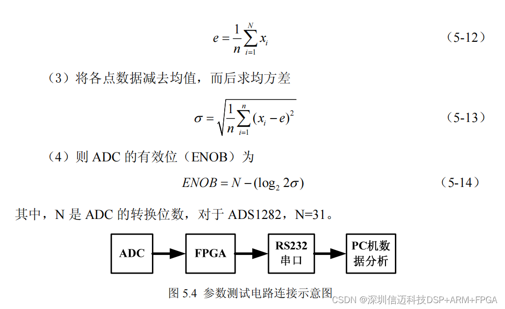
The method for measuring ENOB using the noise floor is as follows: no current signal is applied to the analog front-end; only the inherent noise is digitized. The resulting digital data is collected and sent to a computer for ENOB calculation. The test setup is shown in Figure 5.4, with the following steps [46]:
(1) Acquire n data samples, denoted as x_i, where i = 1, 2, ..., n.
(2) Calculate the mean of the n data points:
Serial data is transmitted to the computer in frame format. A serial reception program saves the received data into a .TXT file. The data frame format is shown in Figure 5.5, where "AA" denotes the frame header, used to distinguish between different data frames. Data1, Data2, Data3, and Data4 together form the 32-bit ADC conversion result, transmitted in big-endian format (MSB first). The interface is shown in Figure 5.6. Each data byte consists of one start bit, eight data bits, one parity bit, and one stop bit, totaling 11 bits. Each data frame contains five such bytes, and 500 frames are transmitted per second, resulting in 27,500 bits per second. Therefore, a baud rate of 38,400 bit/s is selected for serial communication.
5.2.2 ADC Operation Procedure
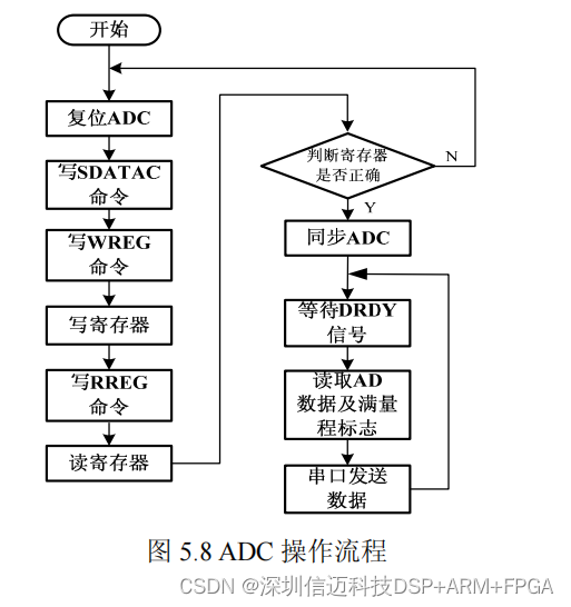
The ADC operation flow during testing is shown in Figure 5.8, and includes the following steps:
(1) Reset the ADC to initialize its internal registers.
(2) Send the SDATAC (Stop Read Data Continuous) command to halt continuous data output from the ADC.
(3) Send the WREG (Write Register) command and write the appropriate configuration data to the corresponding registers.
(4) Send the RREG (Read Register) command to read back the data written in the previous step and verify that it matches the written data. If not, restart from step (1) until successful.
(5) Synchronize the ADC via an external pin to ensure all three ADC channels operate synchronously. Since the ADC is configured in single-synchronization mode, synchronization is required only once.
(6) Wait for the data ready signal (DRDY pin), then read the ADC data via the SPI bus. The data is then formatted into frames and transmitted to the computer via an RS232 serial interface for further analysis. After transmission, return to waiting for the next DRDY signal, repeating the cycle continuously.