【Domestic Virtual Instrument】DSP+FPGA+ADS1282-based 32-Bit High-Precision Data Acquisition Solution (II) Analog Circuit Design
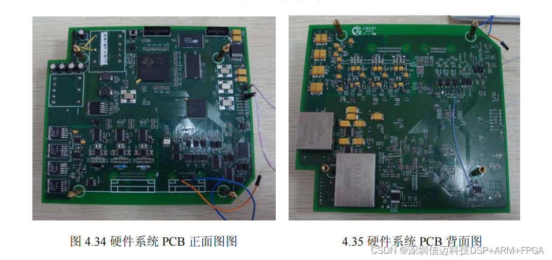
Figure 4.1 shows the signal block diagram of the system hardware. The main core of the digital signal processing board consists of two processing chips: an FPGA and a DSP. The FPGA primarily acts as a bridge between the DSP and peripheral interfaces, and performs data pre-processing, while the DSP serves as the core for data computation.
The FPGA receives data transmitted from external devices via various data buses, performs packaging and other pre-processing, and then stores the data in designated internal memory. The DSP reads the corresponding data via the EMIF bus interface and performs data computation. Parameters and results from the processing are written by the DSP into specified memory within the FPGA via the EMIF bus interface, and then transmitted out by the FPGA via the CAN bus interface.
![](https://pub-048dcb96257f476697b113fcb5939cb9.r2.dev/blog