Implementation Method for ARM+FPGA+AD Multi-Board Multi-Channel Synchronous Acquisition Based on JESD204B Protocol
0 Introduction
With the continuous advancement of digital signal processing technology, the processing of digital signals has become a fundamental method in most current engineering applications. Since analog signals are the original signals in real life, for the feasibility of engineering research, analog signals must be converted into digital signals for processing in engineering. Analog-to-Digital (AD) conversion, as a critical link in converting analog signals to digital signals, has also become an important research subject in engineering [1].
The interfaces of data sampling converters have evolved from traditional CMOS interfaces to differential LVDS interfaces. Due to the low speed of CMOS interfaces, the initial AD sampling rates were limited. Differential LVDS interfaces achieved higher data rate AD sampling. However, with the rapid development of current AD converters, higher sampling rates and higher channel density have become new demands. LVDS interfaces have become somewhat inadequate for this situation. To overcome this challenge, the JESD204B interface emerged.
Currently, there are various radar operating modes internationally, among which array radars have high requirements for synchronization of data sampling between multiple channels, making multi-channel data acquisition an important branch of current data acquisition research. Compared to single-channel AD signal conversion boards, multi-channel AD signal acquisition boards, in addition to evaluating parameters such as effective number of bits (ENOB), dynamic range, maximum sampling rate, and input bandwidth of AD sampling, also need to evaluate amplitude consistency and phase consistency between multiple channels.
This paper describes the design of a multi-channel synchronous acquisition technology for multi-board systems based on the JESD204B protocol.
1 Design Specifications
This paper designs two 4-channel signal acquisition boards to verify multi-board data synchronous acquisition technology.
Each 4-channel signal acquisition board is mainly composed of high-speed AD chips and Field-Programmable Gate Arrays (FPGAs). The AD chip converts external intermediate frequency (IF) signals into digital signals, which are then fed into the FPGA for pre-processing. The FPGA then transmits the pre-processed results to the next-level target unit. The partial design specifications are:
(1) Number of signal acquisition channels: 4; (2) Signal acquisition bandwidth and center frequency: 550MHz ~ 950MHz and 750MHz, respectively; (3) Effective bits: no less than 9.5bit; (4) Signal sampling rate: no less than 1000MSPS; (5) Amplitude consistency between channels: no greater than 0.5dB (R.M.S); (6) Phase consistency between channels: no greater than 5° (R.M.S).
2 Design Process
2.1 Design Principle
After comparing various ADC chips, Analog Devices' AD9680-1000 was selected. This chip has a maximum resolution of 14bit, a maximum sampling rate of 1GSPS, a spurious-free dynamic range (SFDR) of 80dBc (fIN=1GHz), and supports high-speed 2-channel JESD204B serial output. The AD9680-1000 can sample wideband analog signals up to the second Nyquist zone, meeting the requirement for distortion-free sampling of signals in the 550MHz~950MHz range.
To achieve multi-channel AD chip synchronization between multiple boards, TI's LMK04828 clock chip was chosen after comparison. This chip features low RMS jitter, supports the popular JEDEC JESD204B protocol, and can provide up to 14 pairs of differential Device Clocks (including 7 pairs of SYSREF Clocks), which meets the requirements for multi-channel synchronous acquisition across multiple boards.
The principle of multi-channel AD chip synchronization across multiple boards is shown in Figure 1.
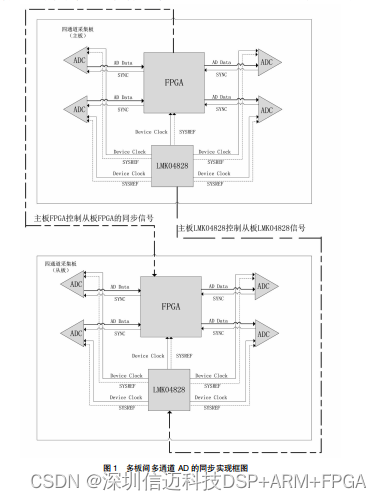
Figure 1 illustrates the synchronous data acquisition of two 4-channel AD boards. One AD board is used as the master board to send control signals and clock reference signals to the other AD board, which acts as the slave board, thereby achieving multi-channel synchronous acquisition between multiple boards.
2.2 Clock Signal
For the master board, both the on-board acquisition clock and processing clock are generated by the LMK04828 clock chip on the master board, and all clocks have a fixed phase relationship. For the slave board, both the on-board acquisition clock and processing clock are generated by the LMK04828 clock chip on the slave board, and all clocks have a fixed phase relationship. Simultaneously, the LMK04828 clock chip on the slave board receives the clock signals and trigger signals generated by the LMK04828 clock chip on the master board. Consequently, the clocks generated by the LMK04828 clock chip on the slave board and the LMK04828 clock chip on the master board also have a fixed phase relationship. Ultimately, all clocks on both boards have a fixed phase relationship, enabling multi-channel synchronous acquisition across multiple boards.
2.3 SYSREF Signal
When using JESD204B technology to achieve delay and synchronous acquisition for multi-channel AD chips, the SYSREF signal is crucial. The generation of the SYSREF signal must satisfy two requirements: setup and hold times relative to the device clock, and operation at an appropriate frequency. Typically, for lower-speed ADC chips, meeting the SYSREF signal's setup and hold times is relatively easy. However, for higher-speed ADC chips, the higher device clock rate reduces the available setup and hold times for the SYSREF signal. In such cases, necessary dynamic delay adjustment may be required to meet timing requirements under different conditions.
SYSREF can be either a continuous or a gapped signal. Its frequency must be equal to the local multiframe clock frequency or an integer division of the local multiframe clock frequency.
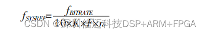
The value of SYSREF can be determined by equation (1). In equation (1), fBITRATE is the bit rate of the serializer/deserializer in JESD204B transmission, K is the number of frames per multiframe, F is the number of 8-bit words per frame, and n is any positive integer [2].
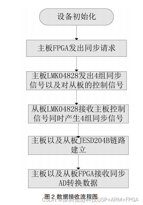
2.4 Synchronous Data Reception Flow
The workflow for multi-channel synchronous acquisition across multiple boards is shown in Figure 2. After the device powers on, all chips on both boards, such as FPGA chips, LMK04828 chips, and AD chips, are configured. Once both boards are configured, the master board first sends out the clock reference signal and synchronous trigger signal. Upon receiving the synchronous trigger signal and clock reference signal, the slave board completes the synchronization timing between the two boards, ultimately achieving multi-channel synchronous acquisition across multiple boards.
3 PCB Design
(1) During PCB design, it is best to allocate a separate, clean, and complete area for the AD working region, providing an independent ground plane to minimize interference from surrounding circuits and improve AD conversion performance [3]; (2) Strictly avoid excessively long AD sampling clock lines to prevent transmission line effects, and ensure the quality of the AD sampling clock; (3) JESD204B data lines can transmit at speeds up to 10Gbps. It is necessary to ensure that the area around the data transmission lines is relatively clean, for example, by prohibiting the placement of crystal oscillators or digital power chips.
4 Design Results
The data converted by the multi-channel AD data acquisition board is first captured into the FPGA for digital signal processing. Based on this, all performance indicators of the multi-channel AD data acquisition board designed in this paper are ultimately derived from testing and calculating the acquired data from the FPGA.
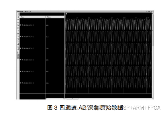
Figure 3 shows a portion of the raw data acquired by the master board's four-channel AD after being captured into the FPGA, obtained using Xilinx's design tool Vivado 2016.4. By analyzing and calculating the obtained raw data, various design specifications for the master board's four-channel AD data acquisition board can be derived. Similarly, various design specifications for the slave board's four-channel AD data acquisition board can be obtained.
5 Conclusion
The multi-channel synchronous acquisition for multi-board systems based on the JESD204B protocol designed in this paper has been successfully implemented. The measured amplitude consistency between multiple channels across multiple boards is less than 0.5dB (R.M.S), and the phase consistency is less than 5° (R.M.S). The effective number of bits for AD conversion on both boards is 9.4bit, which meets the design requirements.
This paper provides a design concept for achieving multi-channel synchronous acquisition between multiple boards based on the JESD204B protocol, which theoretically can be easily extended to achieve multi-channel synchronous acquisition among even more boards.