Hardware Design and Development of an Airborne Radar Servo Control System Based on DSP+FPGA (Part 1) Overall Design
2.1 Functional Requirements and Performance Indicators
2.1.1
Functional Requirements
(1) Capable of two-axis movement (azimuth and elevation);
(2) The azimuth axis can perform preset, continuous scan, and sector scan functions;
(3) The elevation axis can perform a preset function.
2.1.2
Performance Indicators
(1) Motion Range: Azimuth rotation range is , elevation rotation range is ;
(2) Angular Velocity: Maximum azimuth angular velocity is 100º/s, maximum elevation angular velocity is 40º/s;
(3) Angular Acceleration: Maximum azimuth angular acceleration is 90º/s²;
(4) Static Positioning Error: 0.1º (maximum);
(5) Angular Resolution: 0.01º;
(6) System Power Supply: Voltage is 27V, starting current is 6A, operating current is 2.5A;
(7) Electrical Interface: Uses RS-422 transmission protocol, host computer downlink frequency is 100Hz, controller uplink frequency is 200Hz, baud rate is 115200bps;
(8) Environmental Adaptability: Temperature range is −40℃ to 60℃, humidity range is 10% to 90%, altitude greater than 3000m, shock is 25g (11ms);
(9) Features fault feedback, overvoltage protection, overcurrent protection, and power-on self-test functions.
2.2 Overall Scheme of the Airborne Radar Servo Control System
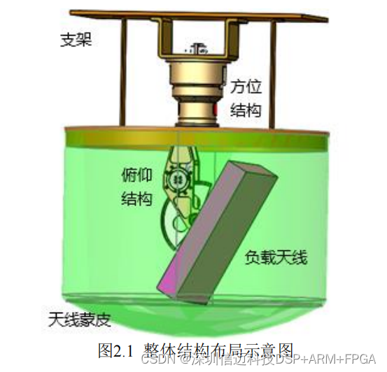
Figure 2.1 shows a schematic diagram of the overall structural layout of the airborne radar servo control system. The upper part is the azimuth section, located between the bracket and the aircraft skin. Inside the azimuth cylinder are components such as a rotary joint, slip ring, azimuth motor, and azimuth angle encoder. The lower part is the elevation section, located inside the radome, containing components such as the antenna, elevation motor, and elevation encoder.
The airborne radar servo control system can be divided into a control unit, a drive unit, and a servo mechanism. The control unit is the key part for realizing servo control functions and is the focus of this paper's design; the drive unit mainly implements power amplification and current sampling closed-loop functions; the servo mechanism carries the antenna load to achieve various functions. The overall scheme design of the system is shown in Figure 2.2:
The control unit in Figure 2.2 is the core of the system, employing a DSP+FPGA combination as the control processor. The DSP is primarily used to implement various control algorithms; the FPGA is mainly used for data interfaces, capable of both data exchange with the DSP via the XINTF interface and generating control timing for peripheral circuits, completing operations such as data acquisition and transmission. This combination fully leverages the advantages of both chips, ensuring timing stability and enhancing the processing speed of control algorithms.
The drive unit is mainly composed of azimuth and elevation axis drivers, which can power amplify the control signals provided by the control unit to drive the motors. The drivers feature over-temperature, over-voltage, and over-current protection functions, as well as fault alarm functions.
The servo mechanism is the executive component of the control system, performing specified functions under the control of the control unit and drive unit. In addition to carrying the antenna load, the servo mechanism also includes components such as motors, angle encoders, slip rings, bearings, and counterweights.
2.3 Control Unit Hardware Circuit Design
2.3.1
Overall Circuit Design
In this servo control system, the control unit is the key design object, and its circuit design scheme is shown in Figure 2.3.
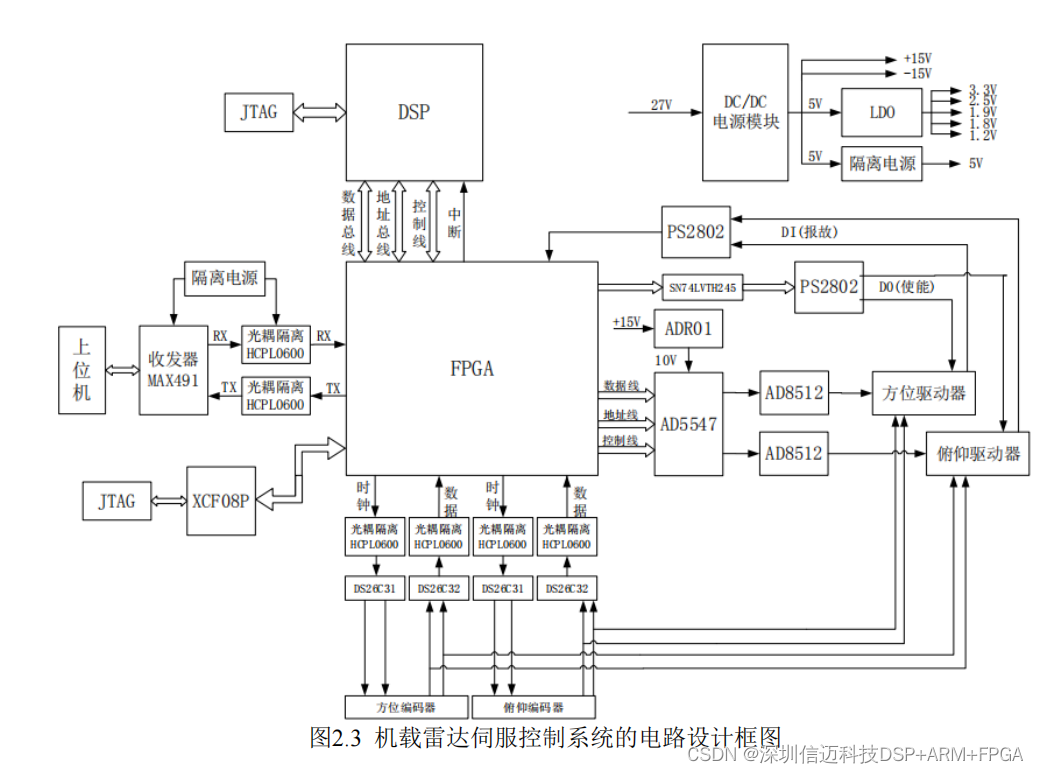
As shown in Figure 2.3, the control processor uses a DSP+FPGA combination, where the DSP primarily implements control algorithms and can exchange data with the FPGA via the XINTF interface. The FPGA is mainly used to implement the control timing of peripheral circuits. Since the FPGA resets after power-off, a configuration chip XCF08P is added to download the program to the FPGA. The remaining circuits are introduced as follows:
(1) The left side of Figure 2.3 shows the host communication interface circuit, implemented jointly by the full-duplex transceiver MAX491 and the optocoupler HCPL0600. To isolate noise interference introduced by the host communication cable, an isolated power supply is used to power this interface circuit.
(2) The bottom of Figure 2.3 shows the SSI interface circuit, used to acquire data from the azimuth and elevation axis angle encoders. The optocoupler HCPL0600 can isolate interference and also perform level conversion. The DS26C31 chip converts the single-ended clock signal output by the FPGA into a differential signal, and the DS26C32 chip converts the differential angle signal returned by the encoder into a single-ended signal. The angle data returned by the encoder needs to be provided to the driver to achieve closed-loop functionality.
(3) The right side of Figure 2.3 shows the drive control circuit, which mainly includes DI/DO interface circuits and a DA interface circuit. The DI circuit is used to receive fault alarm signals output by the driver, and the DO circuit is used to output driver enable and mode selection signals. Both DI/DO circuits use the optocoupler PS2802 for implementation, and the DO circuit adds the SN74LVTH245 chip to enhance driving capability. The DA interface circuit converts the control commands calculated by the DSP into voltage signals and outputs them to the driver. The DA interface circuit is mainly composed of the D/A converter chip AD5547, op-amp AD8512, and reference source ADR01.
(4) The upper right part of Figure 2.3 shows the power supply circuit. The DC/DC power module converts the externally input 27V DC voltage into 5V and ±15V voltages. The 5V voltage is used for digital circuits and is converted to different voltages via various LDO chips; the ±15V voltage is used for analog circuits, powering the op-amp and reference source of the DA interface circuit.
2.3.2
Load Torque Estimation
Load torque is a critical parameter for motor and driver selection. Since airborne radar is subject to vibration and shock, a certain margin needs to be reserved when calculating the load torque. Three types of load torques need to be calculated: inertial torque, friction torque, and unbalanced torque.
2.3.4
Control Chip Selection
The control unit adopts a DSP+FPGA processor combination. The DSP model is TMS320F28335, and the FPGA model is XC4VLX-15.