ZYNQ ARM+FPGA Binocular Stereo Vision Controller Design and Implementation (Part 1)
Implementing a binocular stereo vision system with an FPGA+ARM architecture using a ZYNQ board.
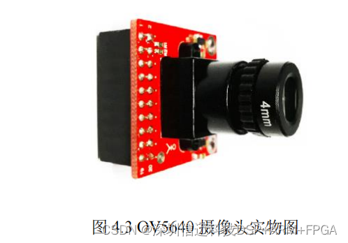
This design utilizes the Zynq-7020 board independently developed by our lab and proposes a hardware and software system design solution for binocular stereo vision based on the FPGA+ARM architecture. Based on the functional division between the system's hardware and software, the PL (FPGA) side primarily handles binocular camera image acquisition, storage, and HDMI display. The PS (ARM) side primarily implements software control, as well as binocular stereo vision stereo matching and stereo rectification algorithms. This design uses an OV5640 binocular camera, with an image resolution of 640480 and an image transmission frame rate of 30fps. High-speed data transfer is achieved via AXI-DMA, and ping-pong operations are implemented using SGI software interrupts and DMA interrupts, ultimately displaying a stable 640480 disparity map on HDMI.
4.1 Introduction to the Binocular System Hardware Platform
4.1.1 Zynq Brief Introduction
Zynq[24] is a new generation of All Programmable SoCs launched by Xilinx. This chip not only integrates a Programmable Logic (PL) system based on Xilinx programmable logic resources but also a Processing System (PS) based on ARM's dual-core ARM Cortex-A9 multi-core processor, as shown in Figure 4.1.
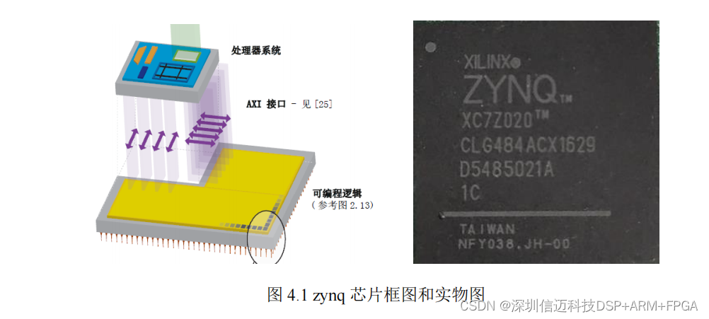
The ARM Cortex A9 multi-core processor is the heart of the PS. It, along with other related processing resources, forms an Application Processing Unit (APU), which supports software programs and operating systems. The PL is essentially a Xilinx FPGA, used to implement high-speed logic[25], arithmetic, and dataflow systems. In Zynq, the PL can be regarded as another reconfigurable "peripheral" of the PS. It can act as a slave device to the PS, controlled by the ARM Cortex A9 multi-core processor. For instance, when the number of serial ports on the ARM Cortex A9 multi-core processor is insufficient, the PL can be used for expansion.
Alternatively, the PL can also be viewed as a master device, not controlled by the ARM Cortex A9 multi-core processor but peer to it, actively performing data interaction with external chips and interfaces. Furthermore, the PL can even act as the master device for the entire system, actively retrieving stored data from the PS's memory and controlling the operations of the ARM processor. Therefore, for Zynq chips, the PS can be used completely independently, without relying on the PL. The PL can also operate independently like the PS, but the limitation is that a JTAG interface must be used to configure the PL. If there is no JTAG interface, the PL cannot operate independently, because both the PS and PL of Zynq must rely on the PS to complete the chip's initial configuration. Although both the PS and PL parts can be used independently, the most valuable mode for Zynq is still to combine and use both the PS and PL parts together.
Since the power supply circuits for PS and PL are designed independently, these two parts can be used separately or together. Compared to traditional FPGAs and ARMs, Zynq All Programmable SoCs not only provide the flexibility and scalability of FPGAs but also offer performance, power efficiency, and ease of use associated with ASICs and ASSPs. This enables designers to implement high-performance and low-cost applications on a single platform using industry-standard tools, such as driver assistance systems, industrial motor control, multi-function printers, professional cameras and machine vision, medical diagnostics and imaging.
4.2 Introduction to Binocular System Peripheral Modules
The core peripheral modules involved in this experimental design include the OV5640 binocular camera, I/O peripheral interface, DDR3 memory, HDMI output, OLED peripheral, and network peripheral modules.
4.2.1.3 Binocular Camera Adapter Board
The expansion ports of the experimental board are shown in Figure 4.8 (a). In this experiment, the adapter board PCB was jointly designed using PADS and Cadence software and sent to the manufacturer for prototyping. The physical prototype is shown in Figure 4.8 (b), and the PADS software design is shown in Figure 4.9.
4.3 Introduction to the Software Part of the Binocular System
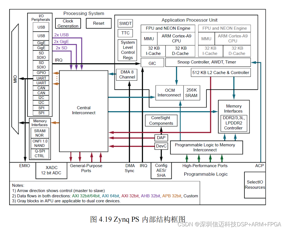
Looking at the overall internal block diagram of the PS, as shown in Figure 4.19 below, the PS can be roughly divided into six parts: 1. Application Processing Unit (APU); 2. AXI Interface (PS-PL); 3. Memory Interface; 4. I/O Peripheral Interface; 5. Clock; 6. Interrupts. Below, I will introduce the content relevant to this experiment.
4.3.1 Application Processing Unit (APU)
The Application Processing Unit is the core of the entire PS. Below, we present the framework structure of the Application Processing Unit, as shown in Figure 4.20.
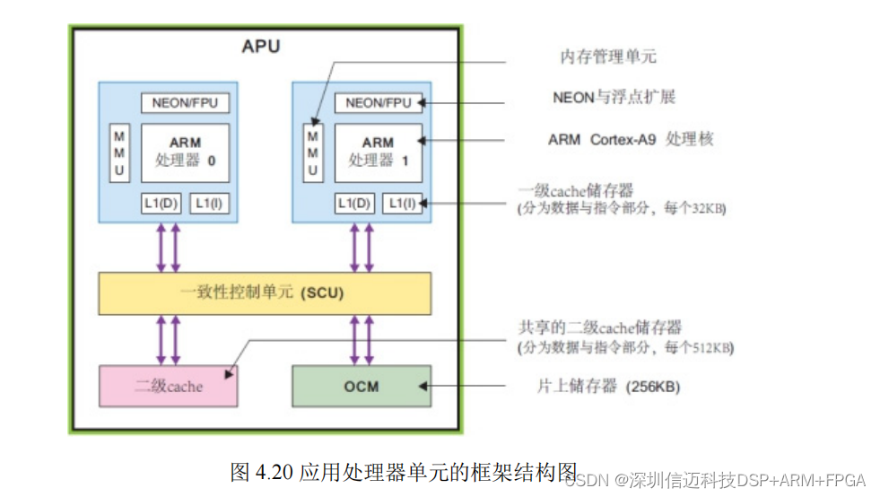
As can be seen from this figure, the Application Processing Unit contains two ARM Cortex A9 processors, each with an independent multimedia processing engine (NEON), Floating Point Unit (FPU), and Memory Management Unit (MMU).
Xinmai provides ZYNQ+Binocular Vision Solutions.