ZYNQ+AD8285 High-Speed Millimeter-Wave Radar Data Acquisition System Design
Traditional millimeter-wave radars employ DSP+FPGA processing modules, where FPGAs enhance data acquisition throughput and DSP devices execute data processing algorithms. To meet the current demands for low power consumption and miniaturization in millimeter-wave radars, while also ensuring data interface stability and speed, this design proposes a ZYNQ-based acquisition system from Xilinx, featuring high integration and high reliability. The PL-side logic resources control high-speed AD data acquisition. The PS-side transmits the acquired data to a host computer, where dynamic parameter analysis of the acquisition system is performed using the Matlab platform. Experiments demonstrate that all dynamic parameters of the AD meet the design requirements, thus validating the rationality of this high-speed acquisition system design.
1 System Overall Design
In millimeter-wave radar applications, the data acquisition system primarily consists of the following components: ADI's 12-bit AD8285, a sampling control module, FIFO, and DMA IP core on the PL side of the Xilinx xc7z020clg400-2, a PS-side Ethernet port, RS485, and a host computer. Figure 1 shows the block diagram of the data acquisition system implementation.
2 AD Conversion Module Introduction
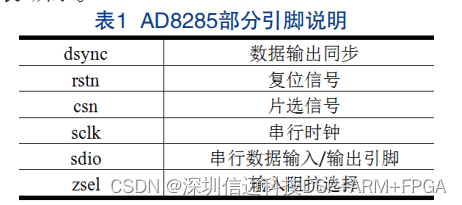
The AD8285 is a low-cost, low-power, four-channel, 12-bit precision high-speed analog-to-digital converter. Each channel has a gain range of 16 dB to 34 dB, and the ADC conversion rate can be up to 72 Msps, with 185 mW per channel (at 12-bit and 72 Msps). In this design, an external 40 MHz crystal oscillator is used to generate a differential clock to drive the AD8285 via the PLL on the ZYNQ's internal PL side. The AD8285 configures its function registers via an SPI interface, with the SPI serial clock set to 5 MHz. Some pin descriptions are shown in Table 1.

On the PL side, a top-down approach is used to design the AD driver circuit in Verilog, comprising the sampling control module, the register function configuration module, and the 3-wire SPI interface module. The sampling control module is responsible for synchronous sampling between the AD8285 and the front-end transmit chip. The register function configuration module performs read/write operations on multiple registers by writing data to addresses via the SPI interface. The 3-wire SPI interface module is a high-speed, full-duplex communication bus, consisting of a serial clock (SCLK), serial data input/output (SDIO), and chip select signal (CSN). In the instruction cycle transfer, the first 16 bits include the R/W read/write indicator bit and W1 and W0 bits controlling the number of bytes transferred, while the latter 8 bits represent the register address. During the data cycle, 8 bits of the value to be written to the register are written [1,2]. The 3-wire SPI timing is shown in Figure 2.
3 Sampling Process Control
In millimeter-wave radar applications, radar Doppler echo data is acquired by the AD8285. This data is transferred to the PS-side DDR3 via the PL-side DMA IP core, utilizing the AXI bus for communication between the PL and PS in the ZYNQ device. Based on the data flow, the DMA IP core is configured to use only the write channel, with other options remaining at default. The PS side uses LWIP and a Gigabit Ethernet port to send the acquired data to a PC for processing. Each time the PL finishes sending a frame of echo data, the DMA IP core generates an interrupt signal. Upon receiving the interrupt signal, the PS sends the DDR3 cached data to the PC via TCP protocol using a ping-pong operation. Additionally, an RS485 serial port is extended in the system for printing debug information. Finally, the test program is solidified using Flash [3].
4 Test Results and Simulation Analysis
ADI provides flexible output test modes for the AD8285. Testing is performed using the Vivado 2017.3 ILA logic analyzer. First, a checkerboard pattern of 101010101010 is output to verify SPI interface communication. Then, the correspondence between multiple channels and data, PGA gain adjustment, and phase differences between multiple channels are analyzed. During testing, an external signal generator serves as the input for the AD8285 acquisition module. The signal generator's host software can set four channels to simultaneously input sine wave signals, and the AD8285's conversion rate, gain, cutoff frequency, and other functions can be configured via the SPI interface.
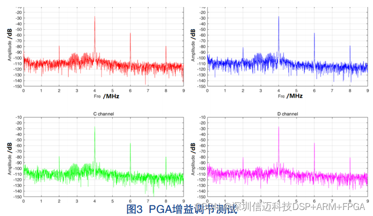
4.1 PGA Gain Adjustment Test
The AD conversion rate is set to 72 Msps. Four channels are fed with the same 4 MHz sine wave signal. The input signal amplitude and phase are consistent for each channel, with full-scale signal amplitude input. Each channel acquires and stores 4096 points. FFT is performed on the 4096 points of each channel using Matlab, and the spectrum curve is recorded, as shown in Figure 3.
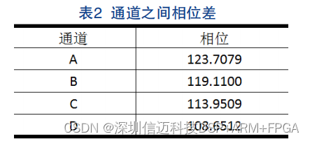
4.2 Phase Difference Test
An external signal generator simultaneously inputs four 1 MHz analog signals to the four channels. All four channels' phases are set to 0 for phase difference analysis. With a 72 Msps conversion rate, the time interval between two adjacent sampling points is approximately 13.8 ns, which corresponds to a phase difference of 5° for a 1 MHz signal. Matlab analysis shows that the phase meets expectations, as shown in Table 2.