Fudan Micro ZYNQ7020 Domestic Replacement Solution Design
The pace of domestic substitution is accelerating. Imported chips were only used for functional verification and will soon be replaced by domestic alternatives. Currently, Fudan Micro is the only domestic company that has developed Zynq-like chips. Shanghai Anlu and Chengdu Huawei are also in the process of R&D (it's not ruled out that Shenzhen Guowei is also working on it, given the significant market potential).
Where are the use cases? First, let's be clear: heterogeneous SoC chips like Zynq (ARM+FPGA) are absolutely not suitable for low-cost solutions. Why?
Using these chips almost always requires accompanying DDR3. The price of a single DDR3 chip is about 100 RMB, and this is for imported ones; domestic ones are even more expensive. As long as DDR is used, at least an eight-layer PCB is required. How much does one PCB fabrication cost? Over 2,000 RMB. If Fudan Micro's FMQL is used, their Nor Flash will be bundled, as other brands are incompatible. Moreover, this Nor Flash is military-grade temperature, costing over 1,000 RMB per chip (imported ones only cost 30 RMB). So, what are the advantages of using such chips?
ARM compilation is fast, while FPGA compilation is slow. If certain early-stage metrics need urgent verification, ARM can be used for rapid validation. ARM is suitable for protocol layer and business layer data parsing, as well as some logic control, because these often require repeated modifications, making ARM very convenient. Portability is also excellent, meaning code can be directly copied from old projects. FPGA is suitable for algorithms and control with strict timing requirements, or high-throughput tasks like data acquisition. Such programs generally don't require major changes in later stages. Due to the chip-level integration, communication between ARM and FPGA becomes very simple, directly using the AXI bus. Compared to routing on a PCB in traditional solutions, this is much faster, better, and more economical. Chip Architecture Differences Unlike Xilinx's dual-core Cortex-A9 + FPGA, Fudan Micro's design features a quad-core Cortex-A7 + FPGA. The FPGA architecture and resources are similar, allowing for almost parallel replacement. On the ARM side, both belong to the Armv7 architecture, a difference akin to two mules versus four donkeys – neither is particularly powerful. Zynq has been around for quite some time; at its release, A9 was considered a relatively new architecture. However, Fudan Micro's FMQL, despite being a latecomer, hasn't surpassed it, and even falls a bit short (Chengdu Huawei's is reportedly a quad-core A53, which is more powerful, and quite anticipated).
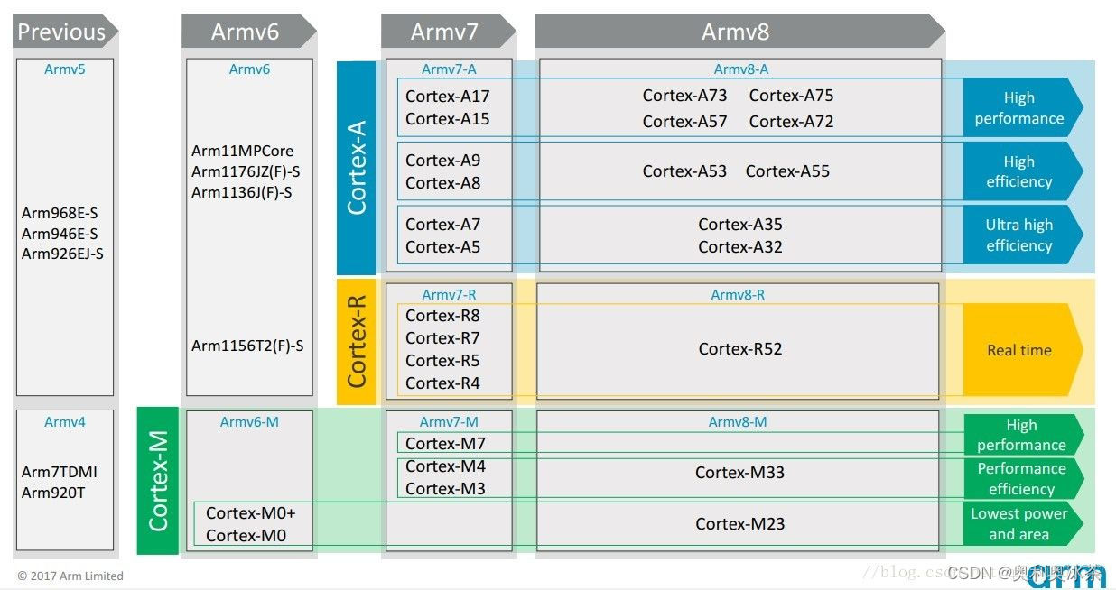
ARM Architecture Diagram
As for why they didn't adopt the same dual-core A9 architecture as Xilinx, I suspect it might be an intellectual property issue. After all, Zynq was jointly developed by Xilinx and ARM. Fudan Micro would inevitably need authorization from ARM to include an ARM core, a hurdle that cannot be bypassed.
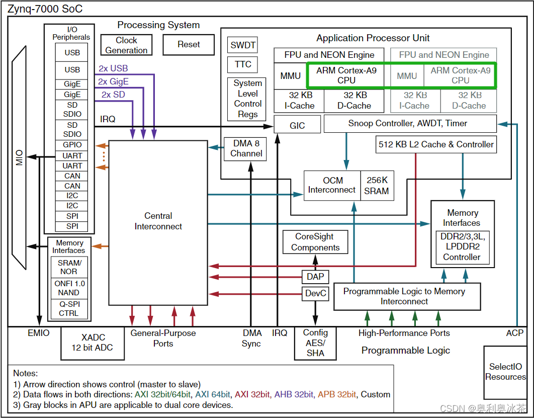
Zynq Chip Architecture Diagram
The different ARM architecture also brings software migration challenges. Zynq uses a customized Eclipse (called SDK) for ARM software development, and with Vivado, the entire ecosystem is relatively closed-loop. Developers don't need to focus too much on low-level details, such as how BSP files are generated or how memory is allocated. However, FMQL has not developed its own IDE, so it uses the IAR development environment, combined with a "lite" version of Vivado software called Procise.
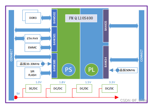
The XM_FDW_ZYNQ7020 is a fully domestically produced core module based on the FMQL20S400. This core module integrates the minimal system of FMQL20S400 (compatible with FMQL10S400) onto a 50*70mm core board. It can serve as a core module for functional expansion, especially leveraging its unique advantages in control applications. The main chip on this core board is compatible with XC7Z020 or XC7Z010 series FPGAs. The core board is equipped with DDR3 SDRAM, EMMC, SPI FLASH, Ethernet PHY chips, and more. PL-side I/O expansion is achieved through two board-to-board connectors. The FMQL20S400 is a fully programmable fusion chip, integrating a feature-rich quad-core processor (PS) and programmable logic (PL) within a single chip. Based on advanced 28nm process technology, and combined with corresponding development software, it creates an integrated hardware and software platform, facilitating development and saving production costs. This core module is primarily used in industrial control signal processing, industrial image processing, and similar scenarios.
Block Diagram
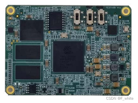
 Physical Photo
Technical Specifications Onboard FPGA Real-time Processor: FPGA Model: FMQL20S400; Processing System (PS): Quad-core processor, maximum frequency 1GHz; Logic Resources: 28K, Block RAM 2.1Mb, DSP Slices 80; Package Size: FCBGA400, 17*17mm, fully compatible with ZYNQ7010;
Dynamic Memory Specifications: Memory Quantity: 2 DDR3 SDRAM chips; Chip Model: SCB13H4G160AF; Memory Bandwidth: 32-bit data bus, operating clock no less than 500MHz; Memory Capacity: ≥2GByte;
Non-Volatile Storage: QSPI FLASH: JFM25Q256, Capacity 256Mbit; EMMC: FEMDRW008G, Capacity 8GByte;
Ethernet Interface: Chip Model: YT8531H;; Supports 10M/100M/1000M auto-negotiating Ethernet;
Other Interface Specifications: Crystal Oscillator: PL side supports 1-way 50MHz clock, PS side supports 1-way 33.33MHz clock; Board-to-board Connectors: 2 x 120-pin located on the bottom layer;
Physical and Electrical Characteristics Board Dimensions: 50 x 70mm Board Power Supply: 1A max@+12V (±5%) Cooling Method: Natural air cooling or metal conduction cooling
Environmental Characteristics Operating Temperature: -40°~﹢85°C; Storage Temperature: -55°~﹢125°C; Operating Humidity: 5%~95%, non-condensing
Software Support Board Support Package (BSP): Supports bare-metal and Linux operating systems; Supports low-level interface drivers; supports peripheral interface expansion; Customizable algorithms and system integration can be provided upon request.
Xinmai provides customized domestic ZYNQ solutions.