Design and Implementation of an Autonomous Driving Domain Controller for Intelligent Vehicles Based on NVIDIA Xavier (Part 1)
Intelligent vehicles play a crucial role in reducing traffic accidents, saving energy and reducing emissions, and alleviating traffic congestion. Autonomous driving systems are the core of intelligent vehicles. In recent years, with the increasing widespread application scenarios of intelligent vehicles, artificial intelligence algorithms have been widely used in autonomous driving systems, and the functions of autonomous driving systems have continuously enhanced. This has led to a situation where the computing power of hardware platforms with a single-chip architecture can no longer meet the needs of autonomous driving systems. The perception system of intelligent vehicles is composed of various types of sensors, which increases the complexity of system integration and communication interfaces. Traditional distributed control system architectures cannot meet reliability requirements. Therefore, designing an intelligent vehicle domain controller with rich interfaces, diverse functions, high performance, and high integration is of great significance.
This paper designs the software and hardware architecture of an intelligent vehicle domain controller system platform based on a heterogeneous chip solution. The hardware architecture uses the CPU + GPU heterogeneous chip module Xavier as the main controller to meet the computing power requirements of multi-sensor fusion perception systems. The external interface design adopts multiple types of interfaces, mainly including multiple Ethernet, UART, and CAN bus interfaces. To reduce the complexity of system integration, the Ethernet interface adopts a non-standard PoE (Power over Ethernet) function design, providing power supply to sensors through the Ethernet interface to reduce wiring. At the same time, the system integrates a combined navigation module and a wireless communication module to provide high-precision positioning and connected communication for intelligent vehicle systems. The software architecture adopts a layered and modular design. The system layer is centered on Linux, integrating ROS middleware and a general software framework to provide distributed communication services and a development framework for the system. The application layer designs general basic software, including data acquisition interface API, vehicle by-wire interface API, map interface API, and combined navigation service API, among others. Compared with traditional distributed controllers, the domain controller designed in this paper features rich interfaces, diverse functions, high performance, and high integration.
2.1.1 Heterogeneous Chip Hardware Architecture
The intelligent vehicle domain controller is a core component that integrates the vehicle by-wire platform and a large number of various peripheral sensors, featuring diverse interface types, sufficient interface quantity, and high performance. Technologies such as multi-sensor data fusion and artificial intelligence algorithms place higher demands on the domain controller's interfaces and computing power. Therefore, the domain controller needs to adopt a hardware solution with heterogeneous multi-core chips that integrate various architectural chips on a single board. The heterogeneous multi-core chip hardware architecture is mainly composed of three parts with different functions: AI units, computing units, and control units, as shown in Figure 2.1.
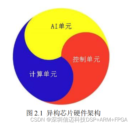
The control unit primarily performs vehicle dynamic lateral and longitudinal control tasks based on traditional vehicle controllers (MCUs). The control unit, equipped with a basic software platform, connects various functional software for vehicle control to achieve vehicle control. At the same time, the software system needs to reserve communication interfaces for integration with the intelligent vehicle operating system.
The computing unit, based on multi-core CPUs, features high clock frequency and strong computing capabilities, managing software and hardware resources and performing task scheduling through the system kernel. The computing unit is mainly used to execute most core algorithms related to autonomous driving, integrating multi-sensor fusion data to complete functions such as path planning and decision control.
The AI unit, based on a parallel computing architecture, is the most computationally powerful part of the heterogeneous chip hardware architecture, allocating and scheduling acceleration engines and software/hardware resources through the system kernel. The AI unit primarily performs analysis and processing of multi-sensor fusion data, outputting surrounding environment information for planning, decision-making, and control. Currently, mainstream AI chip architectures include GPU, FPGA, ASIC, etc., and their performance comparison is shown in Table 2.1.

The CPU primarily performs two tasks: logical computation and control. Among the transistors that make up a CPU, 70% are used to build caches, and the remaining part is used by the control unit to handle complex logic and improve instruction execution efficiency. Therefore, the advantages of the CPU architecture are strong computational versatility, the ability to handle highly complex computations, and low latency. Its disadvantage is relatively low computing power.
A GPU is composed of a large area of ALUs, eliminating complex logical control and focusing on parallel computation of single instructions, making it suitable for large-scale concurrent computing. The advantages of a GPU are simple logical control units and strong parallel computing capabilities. Its disadvantages include smaller cache, higher data read latency, and higher power consumption.
FPGAs are suitable for parallel execution of multiple instructions and single data streams, often used in the "training" phase in the cloud. Because FPGAs lack storage functions, they offer fast computation speed and low operating power consumption, but the overall computational volume is not large. Customers can change their purpose through programming according to actual needs, but mass production costs are higher.
ASIC is a chip architecture that is manufactured to carry only one algorithm for a specific purpose. Initial customization costs are high, but mass production costs are low, and it is suitable for single application scenarios. Currently, autonomous driving algorithms are still rapidly evolving and iterating, making ASICs unsuitable for iterative algorithm development. ASICs will have advantages once algorithms become stable in the future.
For intelligent vehicle systems, a single-chip architecture struggles to meet the demands for processing and analyzing unstructured data such as video, images, and LiDAR point clouds, as well as multi-sensor data fusion. Therefore, intelligent vehicle systems place higher demands on the parallel computing efficiency of in-vehicle processors. Based on the above analysis, the advantages and disadvantages of CPU, GPU, FPGA, and ASIC are compared in Table 2.2.
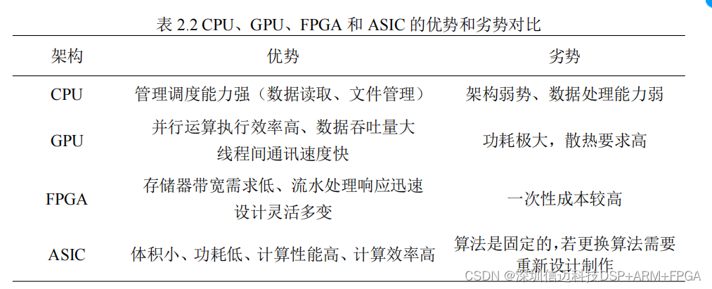
In summary, the compute-to-power ratio of the four chip architectures is ASIC > FPGA > GPU > CPU. While ASICs and FPGAs have higher compute-to-power ratios than CPUs and GPUs, they suffer from higher one-time costs and fixed algorithms. In contrast, the two heterogeneous units based on CPU and GPU still offer advantages. The intelligent vehicle domain controller designed in this paper aims to provide an integrated, functionally diverse, and unified software and hardware interface development platform to support rapid research of various algorithms. A multi-chip architecture based on CPU+GPU is more suitable for the current design requirements of intelligent vehicle system development and algorithm iteration.
Xinmai provides integrated hardware and software solutions for autonomous driving controllers.