VPX Ethernet Switch Board Design Based on Loongson + Domestic FPGA (Part 3)
Debugging and testing are crucial steps in the design and implementation of this system. Single-board debugging primarily involves debugging individual unit circuits and interfaces, mainly by observing signal waveforms and running software to test each function. This chapter will outline a series of debugging and testing plans to verify the correctness of the circuit design.
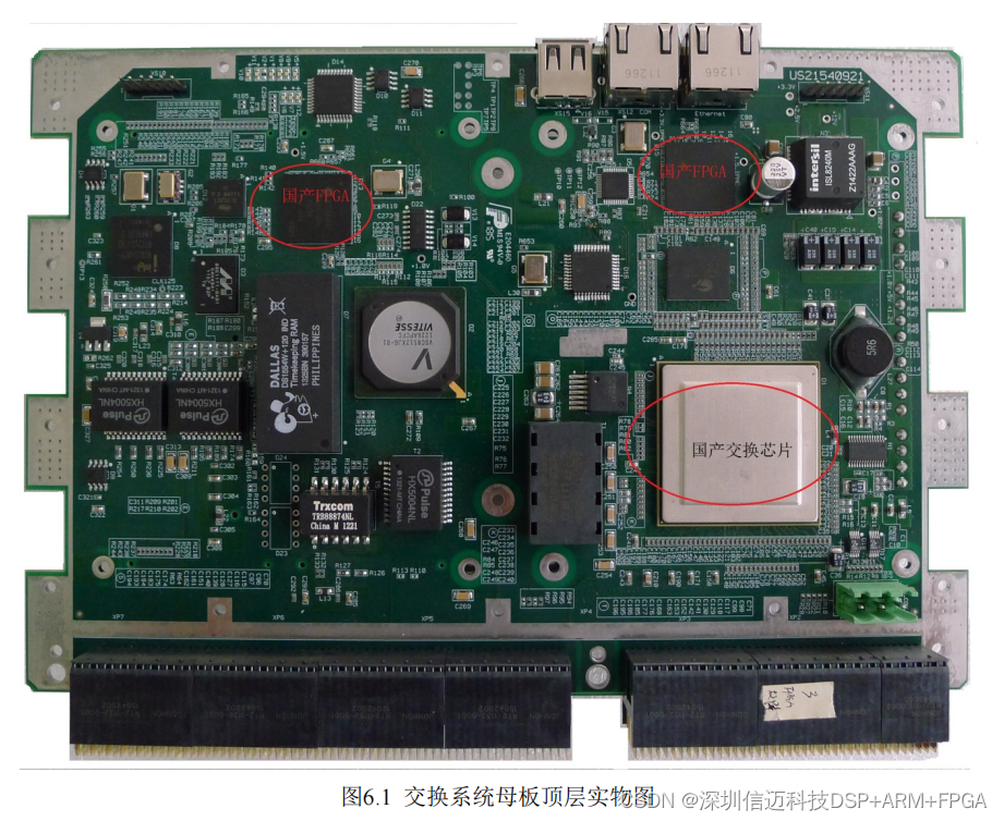
6.1 Circuit Board Static Inspection
After schematic design, PCB layout, manufacturing, and PCB assembly processes, the final circuit board is shown in the figures below. Figure 6.1 shows the top layer of the switch system's mother board, and Figure 6.2 shows the top layers of the power daughter board and CPU daughter board. These two boards are screwed onto the bottom layer of the switch system's mother board.
Before debugging and testing the circuit board, a static inspection is required. This primarily involves checking for open circuits between each output voltage and GND using a multimeter, based on the PCB markings.
![](https://pub-048dcb96257f476697