VPX Ethernet Switch Board Design Based on Loongson + Domestic FPGA (II)
3.1 Board Technical Requirements
3.1.1
Main Performance Indicators
Adhering to the principle of backward compatibility, the design of the Ethernet switch board aims to retain the basic functions and interfaces of traditional information processing platforms, with a focus on improving equipment performance and scalability. The main performance indicators for the Ethernet switch board in this project are as follows:
(1) Features high-capacity, non-blocking switching; switching capacity no less than 16Gbps;
(2) Supports Gigabit optical Ethernet interfaces and electrical Ethernet interfaces;
(3) No packet loss for single-node real-time services, average forwarding delay ≤1ms.
3.1.2
Main Physical Interfaces
In accordance with VPX standard requirements and actual application needs, the main physical interfaces of the Ethernet switch board are as follows:
(1) Provides 20 SerDes interfaces, connected to the backplane connector, providing data exchange for the data plane and control plane via the backplane.
(2) Provides 4 1000BASE-T interfaces and 4 1000BASE-X interfaces, connected to the backplane connector, routed through a backplane adapter board to the device's front panel, providing data access or switch expansion for the device.
(3) Provides a set of serial LED signals, connected to the backplane connector, indicating the status of the front panel data interfaces.
(4) Provides 1 RS232 management serial port and 1 1000BASE-T management network port, simultaneously connected to this board and the backplane connector. The on-board port form is a general RJ45 interface; the backplane side routes through the backplane to the front panel, facilitating debugging of the entire machine.
(5) Provides +3.3V, +12V DC power input interfaces for the board, with interfaces connected to the backplane connector.
3.2 Solution Design
3.2.1
Hardware System Block Diagram
The Ethernet switch board is the core of the information processing platform, mainly comprising two functional modules: central control and core switching. The central control module primarily handles functions such as system maintenance, control, and protocol processing, while the switching module performs the exchange of service data and control information. From a hardware system perspective, the Ethernet switch board mainly consists of the CPU system, CTC6048 switching system, clock and power system, and FPGA processing system. The overall block diagram of the hardware system is shown in Figure 3.1.
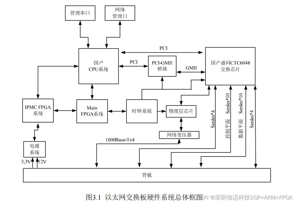
The Centec switching chip provides 24 SerDes pairs to the RT2 connector, of which 4 pairs connect to optical modules for direct output to the front panel, and the remaining 20 pairs are output via the backplane to various service slots, serving as the switching bus for the data plane and control plane, respectively. The switching chip also provides 4 SGMII serial buses, which output 4 10/100/1000 Base-T interfaces to the front panel via external Gigabit Ethernet PHY chips. Data received from the control plane and data plane enters the CTC6048 Ethernet switching chip. After performing Ethernet frame synchronization, FCS verification, packet buffering, and keyword extraction, the chip distinguishes the type of Ethernet frame based on specific fields. For service information, the CTC6048's internal dedicated network forwarding processing engine performs service information classification, network switch table lookup, network switching decision, packet encapsulation, output scheduling, and other processing. For protocol and control information, it is sent to the CPU system via the control channel for processing.
The CPU system uses Loongson 2F as the processor, and then extends necessary interfaces such as management network ports and management serial ports via PCI and LocalBus to achieve management and control of the entire module.
3.2.2
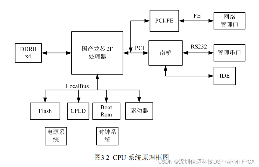
CPU System
The CPU system handles the control and protocol processing of the Ethernet switch board. Its block diagram is shown in Figure 3.2, centered around the Loongson 2F processor, and equipped with BIOS program memory, DDR2 SDRAM memory, a Southbridge controller, reset and control logic, an Ethernet controller, etc. It also extends necessary interfaces such as management serial ports and management network ports via PCI and LocalBus for system debugging and program loading. The clock module provides various clocks required for the normal operation of each chip, including system clock (SYSCLK), memory clock (MEMCLK), PCI interface clock (PCICLK), and four reference clocks for the Southbridge controller: 66MHz, 48MHz, 14.318MHz, and 32KHz. The power conversion module simultaneously provides various power supplies required for the normal operation of each chip.
3.2.3
CTC6048 Switching System
Figure 3.3 shows the data flow diagram for CTC6048 Ethernet data transmission and reception. One Gigabit Ethernet PHY is connected to the CTC6048 via 4 SGMIIs, leading out 4 GE interfaces to the backplane connector, and then through the backplane and front panel adapter board to the front panel of the entire machine. The CTC6048 also directly outputs 28 SerDes pairs, of which 4 pairs go to the backplane P2 connector, through the backplane to optical modules on the front panel adapter board, and then output to the front panel of the entire machine via the optical modules. 10 pairs go to the backplane P2 connector, and 10 pairs go to the backplane P3/P4/P5 connectors, then through the backplane to various service slots, serving as control and data channels for information exchange between service boards. The final 4 SerDes pairs go to the backplane P6 connector, serving as a redundant bus. When the entire machine requires primary/standby switching for increased reliability, these can serve as the information exchange channel for the primary and standby Ethernet switch boards.
Additionally, the CTC6048 communicates with the CPU via a PCI-GMII bridging module, used for transmitting and receiving data packets between the CPU and CTC6048.
3.2.4
Control and Management Channels
The schematic diagram of the control and management channels is shown in Figure 3.4. In the control channel, the processor controls and manages the CTC6048 via a 33MHz PCI channel. The processor also extends a management network port via a PCI-FE bridging chip; a management serial port is extended via a bus bridge chip, then enters the FPGA, where serial port switching is completed within the FPGA. The management network port and serial port are connected to both the on-board RJ45 connector and the backplane connector, outputting to the front panel aviation connector via the backplane. This connection method facilitates both single-board debugging and allows users to manage and configure the entire system after the circuit board is installed in a sealed chassis.
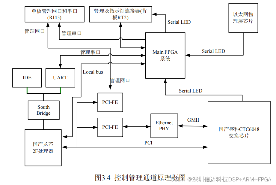
The CTC6048 outputs data that needs to be reported to the CPU for processing via a GMII interface. However, the Loongson processor does not provide a GMII interface, preventing direct connection. The indirect interconnection method is as follows: The CTC6048's GMII interface extends a Gigabit Ethernet port via an Ethernet PHY chip. The Loongson processor extends a Gigabit Ethernet port via a PCI-FE bridging chip. The two Ethernet ports are directly connected, thereby achieving the reporting of protocol data.
Both the CTC6048 and Ethernet PHY provide Serial LED interfaces. By multiplexing within the FPGA, the status of ports to be displayed on the front panel is extracted, then encapsulated into frames, and sent to the backplane connector via the Serial LED interface, finally reaching the panel indicator module via the backplane. The FPGA system is also used to provide reset, clock, port counting, and other functions for each chip. The CPU accesses its internal registers via the Local Bus.
Ethernet Switch Board Solution Implementation
4.1 Characteristics of Domestic Chips
The previous chapter discussed the design scheme of the Ethernet switch board. This chapter first introduces the characteristics of domestic chips, and then elaborates