Application of RK3399+PCIe+FPGA in High-Speed AD Wireless Communication
I. Requirements The requirement is to implement high-speed AD/DA data acquisition and send it to a high-performance ARM core for data processing.
Solution: RK3399+PCIe+FPGA+AD/DA.
II. Device Introduction I. RK3399 The RK3399 is a low-power, high-performance processor for computing, personal mobile internet devices, and other smart device applications. Based on the Big.Little architecture, it integrates dual-core Cortex-A72 and quad-core Cortex-A53 with a separate NEON coprocessor.
Many powerful embedded hardware engines provide optimized performance for high-end applications. RK3399 supports multi-format video decoders, including H.264/H.265/VP9, up to 4Kx2K@60fps. In particular, the H.264/H.265 decoder supports 10-bit encoding, and it also supports H.264/MVC/VP8 encoders at 1080p@30fps, high-quality JPEG encoders/decoders, and special image pre-processors and post-processors.
The embedded 3D GPU makes RK3399 fully compatible with OpenGL ES1.1/2.0/3.0/3.1/3.2, OpenCL 1.2, and DirectX 11.1. A special 2D hardware engine with MMU will maximize display performance and provide very smooth operation.
RK3399 features a high-performance dual-channel external memory interface (DDR3/DDR3L/LPDRDR3/LPDDR4) capable of sustaining demanding memory bandwidth. It also provides a full suite of peripheral interfaces, supporting very flexible applications.
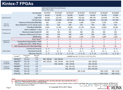
II. FPGA The choice of a pure FPGA is mainly for the logical operations of front-end high-speed AD/DA. Xilinx's 7 series still offers many advantages; it also integrates a PCIe hard core, making it quite suitable for working with RK3399.
Sufficient differential pairs can also meet the interface design requirements of front-end AD/DA.
III. PCIe I. Why PCIe? RK3399 has several dedicated high-speed interfaces, such as MIPI, Gigabit Ethernet, USB3.0, Type-C, eDP, etc. However, for internal communication between on-board devices, dedicated interfaces are limited by protocols and various PHYs, resulting in much less flexibility. For example, high-speed AD/DA data, after being acquired by the FPGA, needs to be transferred to the ARM for data processing. The data format is proprietary and does not conform to MIPI, and trying to adapt it to the MIPI data format would lead to various problems. Therefore, PCIe was ultimately chosen, satisfying both convenience and speed requirements.
RK3399 PCIe features are as follows:
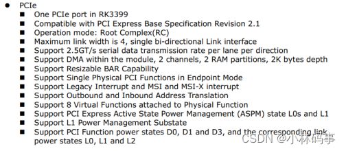
One PCIe port in RK3399
Compatible with PCI Express Base Specification Revision 2.1
Operating mode: (RC)
Maximum link width of 4, single bidirectional link interface
Supports 2.5GT/s serial data transfer rate per lane per direction
Supports in-module DMA, 2 channels, 2 RAM partitions, 2K bytes depth
Supports resizeable BAR capability
Supports single physical PCI function in endpoint mode
Supports legacy interrupts, MSI, and MSI-X interrupts
Supports outbound and inbound address translation
Supports 8 virtual functions accompanying the physical function
Supports PCI Express Active State Power Management (ASPM) states L0 and L1
Supports L1 power management
Supports PCI function power states D0, D1, and D3 and corresponding link power states L0, L1, and L2
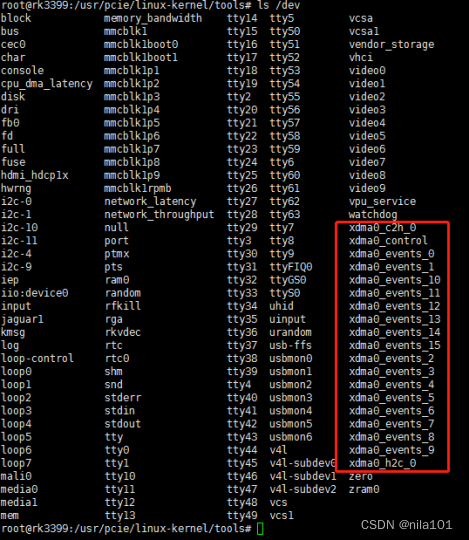
II. PCIe Driver Debugging After correctly generating the FPGA firmware and loading the RK3399 driver, the PCIe device can be seen and called.
root@rk3399:/# lspci -vvv

00:00.0 Class 0604: 1d87:0100

01:00.0 Class 0700: 10ee:9021

root@rk3399:/# lspci -m

00:00.0 "Class 0604" "1d87" "0100" "0000" "0000"

01:00.0 "Class 0700" "10ee" "9021" "10ee" "0007"

root@rk3399:/# lspci -k

00:00.0 Class 0604: 1d87:0100 pcieport

01:00.0 Class 0700: 10ee:9021

root@rk3399:/sys/bus/pci/devices# ls

0000:00:00.0  0000:01:00.0
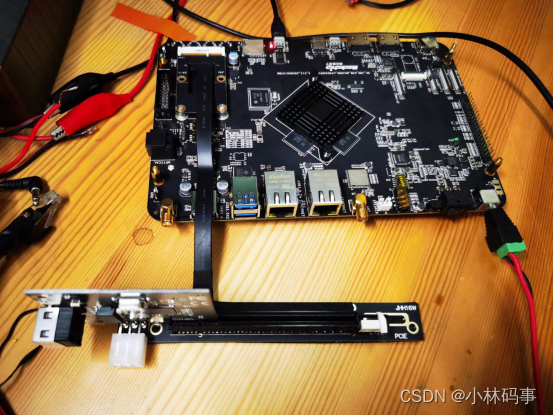
III. Hardware Debugging
Verified as normal through an adapter board from the official development kit, and finally integrated into a single board.