Research on Automated Optical Inspection of PCB Pads and Gold Fingers
Introduction
A Printed Circuit Board (PCB) refers to a designed device that uses insulating material as a substrate, covered with conductive material traces, and without electronic components installed. The function of a PCB is to provide a physical carrier and electrical connections for various electronic components. Modern PCBs are primarily composed of an insulating part made of fiberglass, fabric materials, and resin, along with epoxy resin and copper foil [1-3]. This chapter mainly introduces the current status of PCB defect detection and then summarizes the main research content of this paper.
1.1 Introduction to PCB Inspection
Stability and reliability are important indicators in electronic equipment manufacturing, and the quality of Printed Circuit Boards (PCBs), as core components of electronic products, is extremely crucial. Due to the interaction of various equipment operations and environmental factors during the production process, coupled with the complexity of electronic product manufacturing, different stages in PCB production have a certain possibility of generating various defects such as open circuits, short circuits, voids, residual copper, and scratches. If PCB inspection only begins after components and chips have been mounted or even after assembly into an instrument, it will reduce the yield rate and significantly increase sunk costs [4]. Therefore, it is particularly important to inspect PCBs before mounting and soldering during the production process [5].
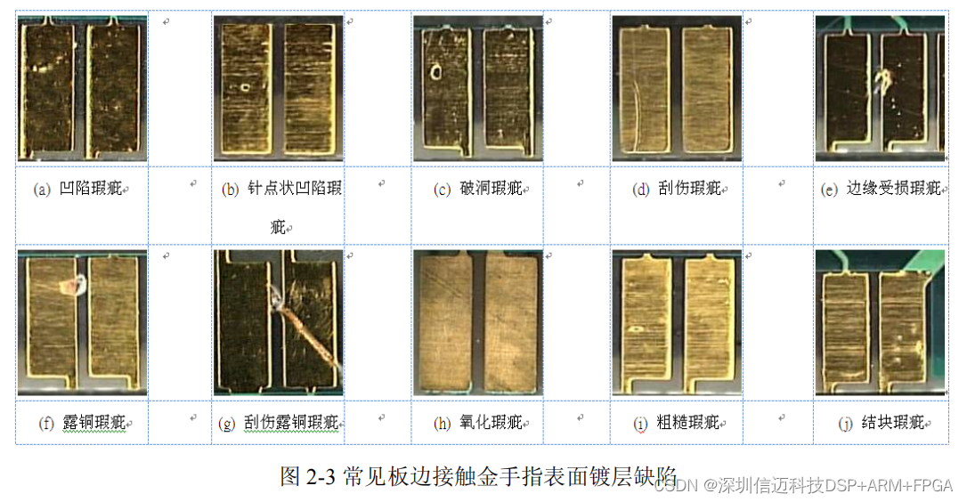
2.1 Introduction to Defects in PCB Pads and Gold Fingers
The inspection standards for Printed Circuit Board (PCB) production are the most important qualitative and quantitative criteria for the entire inspection system. The specific standards for product acceptance are mostly based on the inspection standards of the specific manufacturer. Manufacturers typically formulate their PCB acceptance standards based on IPC-A-600, established by the Association Connecting Electronics Industries (IPC). On this basis, the final PCB acceptance standards are determined by considering the influencing conditions of specific production stages and the parameters required for the final product's electrical connections. During actual PCB production inspection, detected defects need to be labeled with several attributes [32], including:
(1) Defect type, such as incomplete etching.
(2) Defect acceptability status, such as "optimal", "acceptable", "process warning", "non-conforming", etc.
(3) Defect cause, such as process defects caused by improper process modulation or control.
This paper, combining the IPC-A-600 standard and potential defects that may occur during the production process, primarily focuses on researching geometric defects and plating surface defects of pads and gold fingers, while comprehensively considering inspection efficiency, precision, and accuracy.
5 PCB Pad Geometric Defect Detection Based on PCB File Extraction
After image preprocessing to filter out noise and image segmentation, the PCB image under test yields an image where the foreground consists of pads and traces, and the background is the substrate. After image registration, a standard image for information extraction, where all primitives overlap, and an image under test can be obtained. The next step is to perform image defect detection processing on these two binarized images to identify geometric defects in the pads.
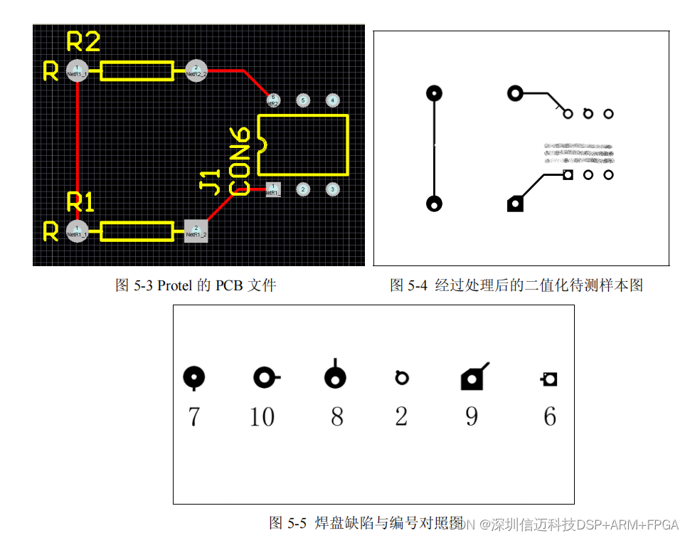
5.1 Analysis of Pad Geometric Defects
Pads are fundamental components of surface mount assemblies, forming the pad patterns on circuit boards that serve as direct connection points between PCBs and electronic components. Their electrical connectivity capability and quality are extremely important, reflected in the pad area, via area, and positional accuracy. Vias in pads are divided into two types: supported and unsupported. Supported vias have a solderable plating inside the hole, while unsupported vias do not. This paper mentioned in the introduction the types of PCB pad geometric defects defined in IPC-A-600, including vias being too close to the junction of the pad and trace. In reality, besides the defect types defined by IPC, there are also defects such as insufficient solder mask area on the pad, undersized vias, and excessively severe via offset.
For pad defect detection, several factors need to be considered:
(1) Detection speed. Since most PCBs are monitored in real-time, after ensuring the speed of image acquisition and stitching, the image detection speed must also be matched.
(2) Detection accuracy. As defect detection uses a standard image extracted from a PCB file as a reference, the detection accuracy can be precise down to the primitive representation unit accuracy of the PCB file. The defect judgment standard during detection can be a direct quantitative unit, determined by the PCB file's units of mil or mm, or by a percentage relative to the corresponding primitive.
(3) Tolerance. Tolerance is a measure to improve the accuracy of defect judgment. Generally, when using a reference standard image to detect geometric defects, it is easy for imperfections within the tolerance range to be mistakenly identified as defects. However, in real-world PCB production inspection, not every discrepancy with the standard image is classified as a defect. To better implement defect judgment conditions in actual production, this paper attempts to introduce tolerance. Based on the acceptance standards proposed by IPC, imperfections within manually set tolerance limits can be accepted.
5.2 Defect Detection Using Correlation Reference Comparison Method
5.2.1 Correlation Reference Comparison Method
The correlation reference method refers to comparing the image under test with a standard image using XOR, OR, AND, and NOT operations. This algorithm is intuitive, simple, fast, and highly implementable. It is suitable for detecting defects such as short circuits, open circuits, and burrs, but it cannot detect excessive or insufficient trace width or spacing, nor can it detect defects on the surface of PCB plating.
In geometric defect detection for PCBs, the logical XOR operation of the correlation reference comparison method is typically used to extract the differing parts between the standard image and the image under test, and then defect types are determined based on the XOR operation process. The operation of the correlation reference comparison method involves aligning the reference points of the registered standard image and the image under test, typically the top-left pixel of the image. Then, both images are simultaneously traversed from top to bottom and from left to right. During traversal, when pixels at the same coordinates in both images are obtained, a logical XOR operation is performed. If the pixels at the same coordinates in the two images are inconsistent, this pixel is set as a flag point. If the pixels at the same coordinates are consistent, the point is set as a background point. After the judgment, the logical XOR operation proceeds to the next pixel. After traversal is complete, the positions of the flag points in the image under test are displayed, and then the location and type of defects are determined based on the flag point positions.