Domestically Produced Fudan Micro FMQL45T900 ZYNQ7045 ARM+FPGA Development Platform
FM4550 Domestically Produced Development Board
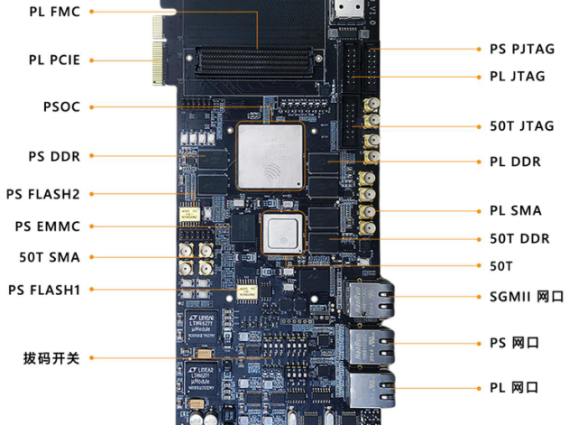
Functional Interfaces -
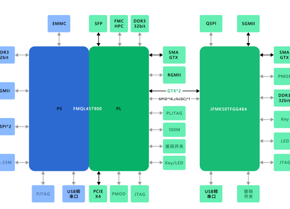
- System Block Diagram -
01
- Product Parameters -
Key Parameters
System 1:
FPGA Model: FMQL45T900
PS Core: Quad-core ARM Cortex-A7, main frequency 800MHz
PS-side Memory: 1GB DDR3, data rate 1066Mbps, 32bit
PL-side Memory: 1GB DDR3, data rate 1600Mbps, 32bit
GTX Transceivers: 16X
Speed Grade: Comparable to imported -2 Chip Grade: Industrial Grade
Operating Temperature: -40℃-100℃ Logic Cells: 350k
Look-Up Tables: 218600 Multipliers: 900
Flip-Flops: 437200 Block RAM: 19.1Mb
EMMC FLASH: 8GB QSPI FLASH: 128Mbit*2
System 2:
FPGA Model: JFMK50TFGG484
PL-side Memory: 1GB DDR3, data rate 1600Mbps, 32bit
GTX Transceivers: 4X
Speed Grade: Comparable to imported -2 Chip Grade: Industrial Grade
Operating Temperature: -40℃-100℃ Logic Cells: 52.16k
Look-Up Tables: 8150 Multipliers: 120
Flip-Flops: 65200 Block RAM: 2.7Mb
QSPI FLASH: 128Mbit
Interfaces and Functions
DDR3:
FMQL45T900:
Two 512MB DDR3 memory chips on the PS side, 32-bit bus, can be used as data cache and operating system runtime memory;
Two 512MB DDR3 memory chips on the PL side, 32-bit bus, can be used for data storage.
JFMK50TFGG484: Features two 512MB DDR3 memory chips, 32-bit bus, can be used for data storage.
QSPI FLASH:
FMQL45T900, two 128Mbit QSPI storage chips on the PS side.
JFMK50TFGG484, features one 128Mbit QSPI storage chip.
EMMC FLASH:
The PS side of FMQL45T900 is equipped with one 8GB EMMC storage chip, which can be used to store the operating system and user data.
PCIe Interface:
FMQL45T900 provides a standard PCIe x4 high-speed data interface, supporting the PCIe Express 2.0 standard.
Ethernet Interface:
Both the PS side and PL side of FMQL45T900 each have one RJ-45 Ethernet interface for Ethernet data exchange.
JFMK50TFGG484 features one RJ-45 Ethernet interface for Ethernet data exchange, using a PHY with an SGMII interface.
JTAG Port:
FMQL45T900 features one PJTAG interface and one PLJTAG interface.
JFMK50TFGG484 features one JTAG port for system download and debugging.
Crystal Oscillator:
The PS side of FMQL45T900 has one 33.333MHz active crystal oscillator, providing a stable clock source for the PS system. The PL side has one 100MHz active crystal oscillator, providing an additional clock for it.
FMC:
FMQL45T900 features one FMC HPC interface, which can connect to various FMC HPC daughter cards. The interface has 6X GTX signals and 84 pairs of differential I/O.
Buttons:
The PS side of FMQL45T900 has one reset button, and the PL side has four user buttons.
JFMK50TFGG484 features four user buttons.
SFP
The PL side of FMQL45T900 has one SFP interface for high-speed optical fiber interconnection.
LED
The PL side of FMQL45T900 has one DONE indicator LED and six user indicator LEDs.
JFMK50TFGG484 features one DONE indicator LED and six user indicator LEDs.
DIP Switch
The PL side of FMQL45T900 has one 4-bit DIP switch.
JFMK50TFGG484 features one 4-bit DIP switch.
Power Parameters
Input Voltage +12V Input Current 2A
Mechanical Dimensions
Dimensions 260mmX111mm
Layers 14-layer board design, ensuring signal quality
02
- Hardware Test Tutorial -
MPSOC PS Test
-
QSPI Loading
-
DDR3 Read/Write
-
EMMC Read/Write
-
Ethernet Port Test (RGMII Interface)
-
USB to Serial Port Transceiver Test
MPSOC PL Test
-
KEY/LED/DIP Switch/PMOD Test
-
DDR3 Test
-
PCIe Test
-
SFP Loopback Test
-
SMA Loopback Test
-
PS to PL LED Test
-
Ethernet Port Test (RGMII Interface)
50T Test
-
QSPI Loading
-
KEY/LED/DIP Switch/PMOD Test
-
Ethernet Port Test (SGMII Interface)
-
SMA Loopback Test
-
DDR3 Test
-
USB to Serial Port Channel Test
MPSOC and 50T Interconnection Test
-
Interconnected GTX Channel Test
-
Interconnected GPIO Channel Test