Design of a Controller for a Semiconductor Motion Stage for Wafer Inspection (Part 2)
Although the overall research and development of precision wafer inspection motion stages in China is currently relatively nascent, it is worth noting that considerable experience has been accumulated in the research of X-Y two-degree-of-freedom motion stages, and even multi-degree-of-freedom motion stages, advanced drive methods, and control strategies. Incorporating this experience into the development of this motion stage will be beneficial for selecting the correct mechanical structure, utilizing advanced drive methods, implementing appropriate control strategies, accelerating project progress, and ensuring project completion. A comparison between standardized precision motion stages from abroad and domestic precision stages is provided below.
Japan has accumulated many years of experience in the manufacturing of precision equipment and holds a leading position internationally. Japanese precision equipment manufacturer THK offers precision XY stages that share many similarities with the motion stage discussed here. These stages are characterized by a rich variety of types, multi-degree-of-freedom travel, and customizable precision, with a typical structure shown in Figure 1-3.
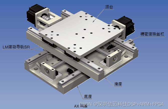
The guide rail section of this stage uses highly reliable LM rolling guides, which can maintain high precision over long periods. Precision ball screws are used for feed, enabling gap-free, accurate positioning. Available travel options include 50mm, 100mm, etc., with a maximum selectable travel of up to 500mm and a maximum load capacity of 250kg. Selectable repeat positioning accuracies are 1µm, 2µm, and 3µm. Optional soft telescopic dust covers are also available. In contrast, although China currently faces many urgent issues in the research and development of ultra-high precision equipment,
and there is still a significant gap compared to developed countries, both in theoretical research and engineering practice. However, with 30 years of rapid economic development since the reform and opening-up, increased domestic and international academic exchanges, the introduction of advanced components, and advancements in theoretical and academic research fields such as electrical control, domestic precision motion equipment has also made significant progress. For example, the three-degree-of-freedom precision motion stage produced by Shenzhen Han's Motor Technology Co., Ltd. in China has achieved precision-level repeat positioning accuracy (±2μm), as shown in Figure 1-4.

The LMSU13 platform uses coreless LSMU series linear motors as direct drive components for linear motion, and DDR series rotary motors as direct drive components for rotary motion. Utilizing an incremental optical feedback system, this three-dimensional stage features a compact structure, no mechanical contact, low noise, long lifespan, no mechanical transmission links, high-speed response, short acceleration/deceleration times, and can be fitted with an enclosure, making it suitable for high-precision inspection and positioning applications. Its main technical specifications are:
(1) Maximum travel: 250mm * 300mm * 360°;
(2) Repeat positioning accuracy: Linear ±2μm, Rotary ±2 arcseconds;
(3) Three-dimensional dimensions: approximately 516mm * 650mm * 356mm;
(4) Linear motor peak thrust: 308N, Rotary motor peak torque: 17Nm.
Overall Design of the Wafer Inspection Motion Stage
Drawing from the experience with advanced wafer inspection motion equipment abroad, it is known that the wafer inspection process requires the use of multi-degree-of-freedom precision motion stages, which typically come in two main types: three-degree-of-freedom and four-degree-of-freedom. Three degrees of freedom generally refer to R, Z, and theta, while four degrees of freedom generally refer to X, Y, Z, and theta. This chapter first introduces the basic principles and procedures of wafer inspection, analyzes the performance parameter requirements for the motion stage across multiple degrees of freedom, and then, based on this requirements analysis, proposes an overall machine design solution, which is described from the perspectives of mechanical structure design and control system design.
2.1 Design Requirements and Technical Parameters
2.1.1 Principle of Wafer Inspection Motion
The primary application of multi-degree-of-freedom precision wafer inspection motion stages is the detection of chemical particulate contaminants on wafer surfaces, with the main targets being chemical particulate contaminants ranging from 30nm to 100nm in diameter [17]. Its basic working principle involves using an optical lens to perform a comprehensive "carpet-style" scan of the wafer surface, observing and recording the morphology and position of chemical particulate contaminants in an imaging system. It also requires the control system to accurately determine and record the coordinates of these contaminants across the entire wafer until the entire surface is scanned. As is well known, a complete scan of a circular plane can be achieved using either a raster scan or a spiral scan. This paper compares the different requirements these two working methods impose on the motion stage. The three-degree-of-freedom motion stage relatively offers the following advantages: (1) Three degrees of freedom require one less degree of motion than four degrees of freedom, which can save costs; (
- Eliminating one linear motion axis can reduce the overall height of the motion stage, increasing its structural compactness and better ensuring precision;
(3) Spiral scanning can be more efficient than raster scanning.
Therefore, this paper designs the motion stage based on a three-degree-of-freedom spiral scanning working method.
The basic working principle of the three-degree-of-freedom precision wafer inspection motion stage is as follows: an optical lens, using a spot size of 50µm (or 100µm, 150µm, etc.), scans along an Archimedean spiral, as shown in Figure 2-1, to detect chemical particulate contaminants within a specified area on the entire wafer surface. The Archimedean spiral scanning motion is formed by superimposing a constant velocity linear feed motion along the wafer's radius R and a constant velocity rotational motion around the wafer's center (Theta axis). The resulting Archimedean spiral is shown in Figure 2-1.

Taking scanning with a 50µm diameter spot as an example, the Archimedean spiral motion generated by superimposing constant linear motion and constant rotational motion can cover the entire surface of the wafer. Simultaneously, the constant linear feed speed of the wafer along the radius R corresponds to a linear feed amount of 50µm per revolution of the wafer (or the diameter of other detection spots). From this, it can be concluded that this is a typical and commonly used basic method for detecting chemical particulate contamination on wafers. In this mode of operation, there is a specific correspondence between the rotational speed and the linear motion speed, i.e., the linear motion speed is 50µm/revolution. Furthermore, there are currently detection methods that use multiple spots for simultaneous inspection. Their basic working principle is similar to the single-spot detection described previously, with the difference being the use of multiple spots to inspect the wafer concurrently, which can significantly improve wafer inspection efficiency.