RF Solution Based on AD936X and Intel FPGA
An RF solution based on ADI AD936X and Intel Cyclone V FPGA is suitable for applications such as wireless communication infrastructure, defense electronics systems, RF test equipment and instrumentation, and general-purpose software-defined radio (SDR) platforms.
About the ADI AD936X Series RF Transceiver
The AD936X series operates over a frequency range from 70 MHz to 6 GHz. It is a complete radio design, a single-chip integrated solution. It integrates multiple functions, including an RF front-end, mixed-signal baseband section, frequency synthesizer, analog-to-digital converter (ADC), and direct conversion receiver. The AD936X supports channel bandwidths from below 200 kHz to 56 MHz, offers high programmability, boasts an unparalleled dynamic range in today's market, and provides leading noise figure and linearity performance, as well as an economical and low-power radio solution.
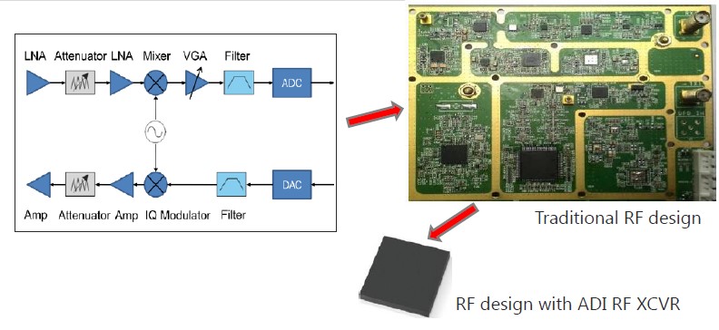
Figure 1: Traditional RF design integrated into a single AD936X chip
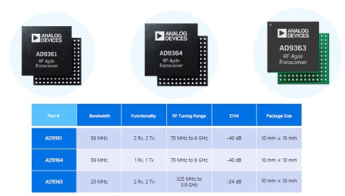
Figure 2: Parameter specifications for the three chips in the AD936X series
About the Intel Cyclone V Series FPGA
Intel's Cyclone® V FPGAs are developed using TSMC's 28-nm Low-Power (28LP) process, achieving the industry's lowest system cost and power consumption. Their performance level makes this device family an ideal choice to highlight the advantages of your high-volume applications. Compared to previous generations, total power consumption is reduced by 40%, offering efficient logic integration capabilities, and providing models with integrated transceivers as well as SoC FPGA models featuring an ARM-based Hard Processor System (HPS).
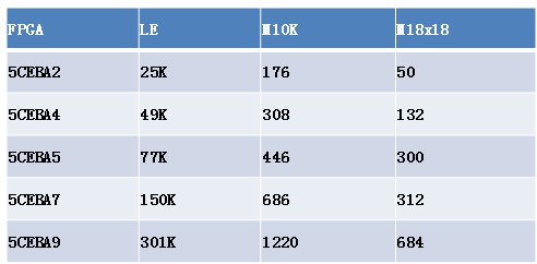
Figure 3: Cyclone V E FPGA Parameters
Full-Band RF Development Platform
The programmable full-band RF development platform board is shown in Figure 4:
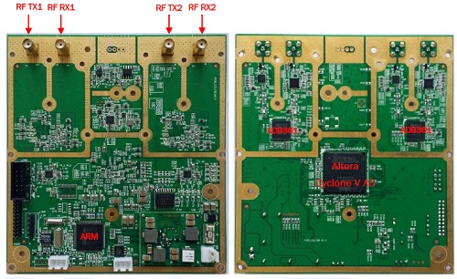
Figure 4: Full-Band RF Development Platform (Front and Back)
- RF Section: Utilizes ADI's most advanced RF Transceiver, the AD9361. The entire RF section offers the highest integration, lowest power consumption, and greatest flexibility, supporting bandwidths from 200 kHz to 56 MHz and an RF transmit/receive frequency range from 70 MHz to 6 GHz.
- Digital Signal Processing Module: Employs an Intel Cyclone V series FPGA (A5 by default), featuring rich DSP and logic resources, while also compatible with A2/A4/A7 and A9 variants, allowing customers to choose according to specific project requirements.
- Main Control Unit: The development platform uses an STM32 series general-purpose MCU to implement monitoring and network management functions.
RF Module
The RF module board outline and schematic block diagram are shown in Figures 5 and 6. The FPGA used is 5CEBA5F23C8N (compatible options like 5CEBA2, 5CEBA4, 5CEBA7, 5CEBA9 can be selected based on customer needs). The RF XCVR (transceiver) used is AD9361 (compatible options like AD9363, AD9364, etc., can be selected based on customer needs). The module size is credit card-sized.
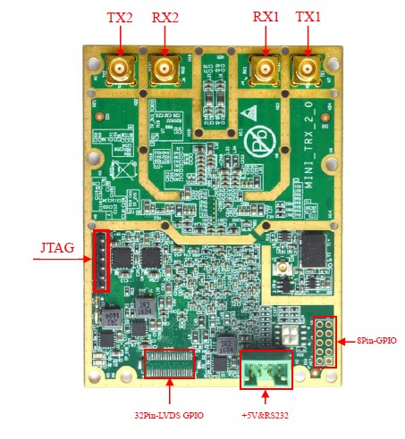
Figure 5: RF Module Board Outline
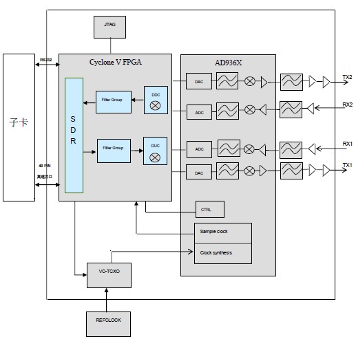
Figure 6: RF Module Schematic Block Diagram