SI+PI Co-Simulation Analysis of DDR3/DDR4 for Domestic DSP+ARM+FPGA Chips
Simulation for Domestic DSP + ARM + FPGA Chips
Simulation Targets: DDR2/3/4/5, LPDDR2/3/4/5, etc.
● SI/PI co-simulation, batch simulation
● Participation in industry standards development for DDR3/4/5 design
● Simulation vs. test correlation to improve simulation accuracy
● Extensive DDR3/4/5 product debug experience
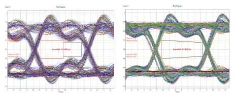
Signal Quality Simulation
- Comparison of results before and after simulation optimization
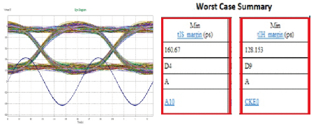
Timing Simulation Analysis
- Timing relationship across signal groups
- Timing window calculation (setup/hold time margin)
Simulation Challenges
High routing density, large number of components, high operating speeds, tight timing margins, and multiple driver types.
Simulation Scope
Topology optimization, ODT tuning, driver selection, termination and series resistor value adjustment, timing analysis, full-channel simulation for all signal lines.
Simulation Objectives
- Perform pre-layout simulation to derive design rules and guide layout placement and routing
- Conduct post-layout simulation to verify correctness and rationality of the layout
- Identify and resolve issues during project debugging by simulation-based root cause analysis and improvement recommendations
- Simulate internal chip signals that cannot be measured directly, by correlating with external test data to model true internal behavior
Simulation Significance
- When layout and routing conditions fail to meet design requirements, simulation objectives become clearly defined
- Selection of DDR3/4/5 topology types (fly-by, T, or hybrid fly-by+T) based on design constraints
- Evaluate whether ODT can be disabled while maintaining stable operation under low-power requirements
- Provide design guidance for high-density, cost-reduction scenarios (e.g., layer reduction, use of standard materials)
- Offer routing guidance for HDI designs with incomplete reference planes or poor length matching capabilities