Image Recognition Hardware Design and Algorithm Implementation Based on Domestic Galaxy Phytium Multi-core DSP + FPGA
With the development of surveillance satellites, how to quickly identify targets in satellite images has become a key technology. To achieve the localization of key on-board components and provide higher performance and better real-time capabilities for the entire system, this project will use the high-performance multi-core DSP chip independently developed by the College of Computer Science, National University of Defense Technology, as the processing core, supplemented by an FPGA, to build an image acquisition and recognition hardware processing platform, and research and implement ship target recognition algorithms on this platform.
Main work: ① Design a processing framework based on Phytium multi-core DSP+FPGA. This framework fully utilizes the DSP's ability to process digital signals and the FPGA's ability to control interfaces. It features a flexible structure and meets design requirements for small size, low power consumption, and fast processing speed. ② Complete the hardware circuit design for the entire platform. ③ Complete the debugging of each functional module. The FPGA can achieve image acquisition and display, extract valid image data from the acquired information, perform grayscale processing on the images, and realize data transmission and communication with the DSP. The DSP can communicate with the host computer. ④ Use algorithms based on grayscale thresholding and effective edge information to identify ship targets, determine the relative position of targets in the image, and display the processing results on a display device. ⑤ Optimize the program for multi-core processing based on the characteristics of the Phytium multi-core DSP to improve program efficiency.
The designed hardware platform can achieve image acquisition and processing, identify ship targets under general conditions, and display the results on a display device.
The high-performance multi-core processor FT-XXX, independently developed by the Institute of Microelectronics, College of Computer Science, National University of Defense Technology, has a digital signal processing capability 1 to 2 orders of magnitude higher than general-purpose microprocessors at the same operating frequency, and its power consumption is 1 to 2 orders of magnitude lower. In modern warfare, it is necessary to process and analyze critical information promptly. Therefore, Phytium DSPs are widely used due to their powerful digital signal processing capabilities, covering application areas such as precision guidance, radar signal processing, secure communication, flight control, electronic countermeasures, and sonar detection. They are one of the most urgently needed core components in the development of information processing systems.
Currently, Galaxy Phytium DSPs have been applied in various fields, such as image acquisition and processing for unmanned aerial vehicles, control devices for artillery systems, and underwater information processing systems. This is the first time a Phytium multi-core DSP has been applied to a satellite. Researching an on-board image acquisition and recognition platform will broaden the application scope of Galaxy Phytium DSPs, obtain the working status and capabilities of Phytium chips in a real space environment, accumulate experience for system-level design in space environments, and verify whether Phytium chips can meet design requirements in practical applications.
At the same time, researching the application of Phytium multi-core DSPs on satellites is conducive to achieving the localization of satellite core components, which is of great significance for information security.
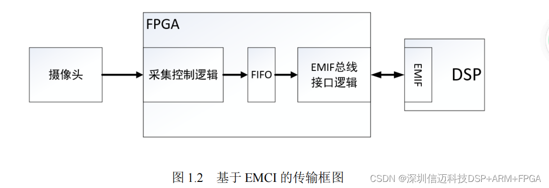
An embedded strapdown navigation system [5], its block diagram is shown in Figure 1.3. In this design, the FPGA stores the acquired image data into SDRAM after preliminary processing, and simultaneously stores the data into dual-port RAM. Dual-port RAM is fast, real-time, and easy to operate. The DSP reads data from the dual-port RAM via EMIF. This design can not only store multiple frames of images but also meet the requirements for fast data transfer between the DSP and FPGA. The drawback is the need to select an FPGA model with sufficient memory resources.

The FPGA+DSP image processing architecture [6,7] makes image processing platforms more portable, lower power, and higher performance, and this architecture is continuously developed and optimized [8,9]. This paper combines the characteristics of Phytium DSPs and aims for space deployment, designing a more powerful and stable image processing hardware platform, while also implementing and improving it.
Hardware Circuit Principle Design
The image processing platform based on Phytium multi-core DSP+FPGA is shown in Figure 2.1. This platform mainly includes four key modules: image input module, image pre-processing module, image processing and storage module, and image display module. Figure 2.1 shows the interfaces used in the actual application of this project, while other functional interfaces are also reserved in the overall board design, including a hard disk storage interface reserved in the FPGA section for storing received raw images, and an SRIO interface reserved for communication between the FPGA and DSP in addition to the HPC bus and EMCI bus. These will be introduced in detail in later chapters. This paper will individually introduce the working principles and implementation of each module, as well as the overall system workflow and effects.
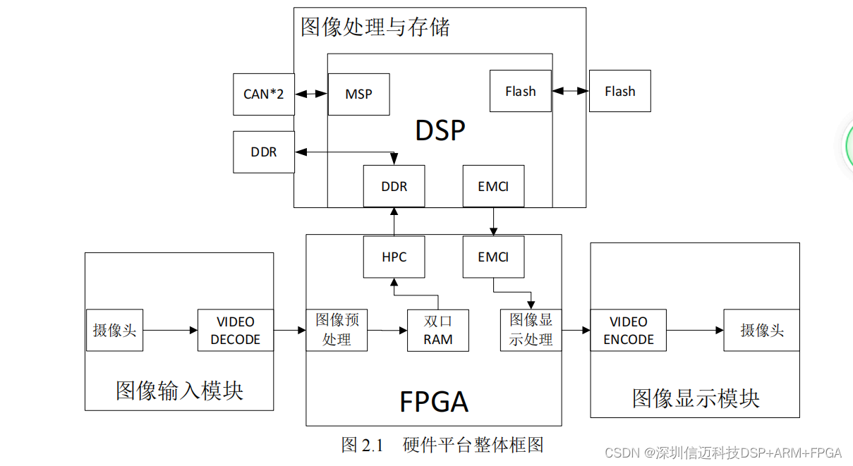
As shown in the overall block diagram in Figure 2.1, the camera acquires images, and then an A/D conversion chip converts the video signal into a BT.656 format digital signal. After the digital image signal enters the FPGA, it first performs a blanking signal removal operation on the BT.656 format image, retaining only valid data, and then stitches the valid data into a complete image. The FPGA stores the image data in RAM. Internally, the FPGA implements HPC interface logic using hardware description language, connecting to the DSP's HPC interface, and transfers data to the DSP's DDR2 space via the HPC bus protocol. Before receiving image data, the DSP needs to configure DDR2 to ensure its normal operation. The DSP processes the image, identifies ship targets using recognition algorithms, determines the relative coordinates of the ships in the image, and then transmits the coordinate information to the FPGA via EMCI. After the FPGA receives the coordinate information, it combines it with the original image, then transmits the image information to a video decoding chip, which then displays the original image and a crosshair indicating the ship's relative position on the output display device. Simultaneously, the DSP communicates with the CAN chip via Mfsp, and the CAN chip communicates with the satellite via the CAN bus.
Overall Hardware Design Framework
After determining that the overall hardware platform will be an FPGA+DSP architecture, a detailed design of the entire hardware platform is required. The design goal is a ship target recognition system to be deployed on a satellite, so the primary considerations during the design process are system stability, improving system performance while maintaining stability, and reducing overall power consumption.
In designing the entire hardware platform, the entire hardware circuit can be divided into the following parts: clock circuit, power supply circuit, reset circuit, image acquisition circuit, image display circuit, DSP-FPGA communication circuit, DSP-CAN chip communication circuit, DDR2 storage circuit, etc. The circuit schematic diagram is shown in Figure 3.1.
![](https://pub-048dcb96257f476697b113fcb5939cb9.r2.dev/blog/126966000/05_13d5bdf50e9dc08d9a63