Physical Vapor Deposition Semiconductor Equipment PVD DSP/ARM+FPGA Controller Design
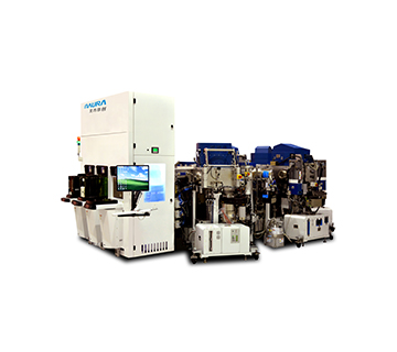
Magnetron sputtering technology is a type of PVD (Physical Vapor Deposition) technology and one of the important methods for preparing thin film materials. It utilizes the characteristic that charged particles gain kinetic energy after being accelerated in an electric field, directing ions towards a target electrode (cathode) made of the material to be sputtered. This process sputters target atoms, causing them to move in a specific direction towards a substrate and deposit as a film on the substrate. Magnetron sputtering equipment allows for controllable film thickness and uniformity, producing films with good density, strong adhesion, and high purity. This technology has become an important means for preparing various functional thin films. Naura Akrion has made breakthroughs in several key technologies, including sputtering source design, plasma generation and control, particle control, chamber design and simulation, and software control. This has established core technological advantages with independent intellectual property rights, achieving a breakthrough in high-end thin film deposition equipment for the domestic integrated circuit industry. Its equipment applications span multiple technology generations, representing a high level of domestic integrated circuit thin film process equipment, and have successfully entered the international supply chain system. Naura Akrion has successively developed and successfully commercialized multiple PVD products with independent intellectual property rights in fields such as integrated circuits, advanced packaging, and LEDs.
As a process step in integrated circuits, Al Pad PVD plays a crucial role in connecting to subsequent packaging processes. In integrated circuit manufacturing, almost all semiconductor devices utilize Al Pad PVD for their backend metal interconnects, providing electronic signals and micro-connections for various components within the chip. The Al Pad Physical Vapor Deposition system is an important process step in integrated circuit manufacturing, primarily applied in bond pad and Al interconnect processes. Currently, the typical Al pad process uses an Al thickness of 1um. With the development of integrated circuit technology, Al Pad thickness is increasing, especially for technology nodes below 28nm, where 3um thick aluminum applications are gradually becoming mainstream. This change places higher demands on equipment for high throughput, high efficiency, low cost, and low defects. To better adapt to the rapid development of the semiconductor market, Naura Akrion timely launched the eVictor A830 Al Pad Physical Vapor Deposition system in early 2015, a product with numerous features.
1 Evaluation Board Introduction Based on TI KeyStone C66x multi-core fixed/floating-point DSP TMS320C665x + Xilinx Artix-7 FPGA processor; TMS320C665x main frequency is 1.0G/1.25GHz, with single-core computing capability up to 40G MACS and 20G FLOPS. FPGA XC7A100T has 101K logic cells and 240 DSP Slices; TMS320C665x and FPGA are connected via communication interfaces such as uPP, EMIF, I2C, PCIe, and SRIO, with PCIe and SRIO each supporting a maximum transmission speed of 5 GBaud; The FPGA acquisition card supports dual-channel 250MSPS12Bit high-speed high-precision ADC, and one-channel 175MSPS12Bit high-speed high-precision DAC, meeting various data acquisition requirements; Supports Gigabit Ethernet port, connectable to industrial network cameras, and also supports common interfaces such as I2C, SPI, UART, McBSP; Supports expansion modules such as CameraLink input/output and VGA output; Supports bare-metal and SYS/BIOS operating systems.
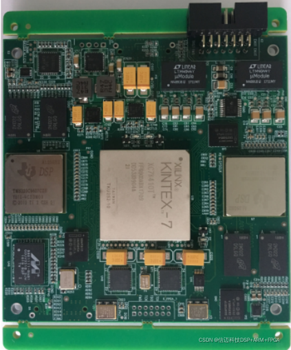
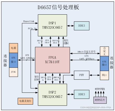 Figure 1: Development Board Physical View
Shenzhen Xinmai's XM-C665xF-EVM, based on TI's design, is a DSP+FPGA high-speed big data acquisition and processing architecture, suitable for high-end image processing, high-speed big data transmission, and audio/video big data acquisition and processing fields. This design combines the board cards through communication interfaces such as uPP, EMIF, I2C, PCIe, and SRIO of the TMS320C665x, forming a DSP+FPGA architecture, achieving a unique, flexible, and powerful DSP+FPGA high-speed data acquisition and processing system.
The SOM-XM665xF exposes all CPU resource signal pins, making secondary development extremely easy. Customers only need to focus on upper-layer applications, reducing development difficulty and time costs, enabling rapid product launch and timely seizing of market opportunities. It not only provides rich demo programs but also offers DSP inter-core communication development tutorials and comprehensive technical support to assist customers with baseboard design and debugging, as well as multi-core software development.
2 Typical Application Areas Data Acquisition, Processing and Display System Telecom Tower: High-speed data acquisition and generation for Remote Radio Units (RRU) High-speed Data Acquisition and Processing System High-end Image Processing Equipment High-end Audio and Video Data Processing Communication Systems 3 Software and Hardware Parameters The front end uses FPGA to acquire two channels of AD data, which is then transmitted to the DSP via communication interfaces such as uPP, EMIF bus, or PCIe, SRIO interfaces. After AD data is processed by the DSP, it can be used for applications such as data comparison and analysis, network forwarding, and SATA hard disk storage. Based on the processing results, the DSP sends the obtained logical control commands to the FPGA, which then controls the onboard DA to achieve logical output with an update rate of 175MSPS.
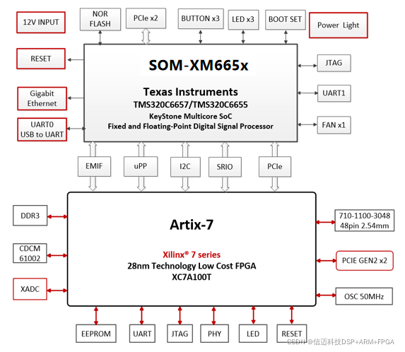 Figure 2: Big Data Acquisition Block Diagram
The high-speed data acquisition front-end consists of an FPGA synchronously acquiring two channels of AD analog input signals, enabling pre-filtering of AD data, with an AD sampling rate up to 250MSPS. Another DAC channel can output parallel DA data of arbitrary amplitude and waveform, with an update rate of 175MSPS. The high-speed data transmission section is composed of communication interfaces such as EMIF, I2C, PCIe, and SRIO. Large-throughput AD and DA data can be transmitted stably and at high speed between the DSP and FPGA via SRIO and PCIe interfaces; the DSP can perform logical control of the FPGA and exchange medium-throughput data via the EMIF bus, and also perform initialization settings and parameter configuration for the FPGA via I2C. (3) The high-speed data processing section consists of the DSP core and algorithm library. It can perform real-time transformation processing of signal parameters such as time domain, frequency domain, and amplitude for AD and DA data (e.g., FFT transform, FIR filtering). (4) The video acquisition and output expansion section is composed of CameraLink input/output modules, VGA output modules, Gigabit Ethernet, and other components. With rich interface resources and flexible and convenient solution selection, it is an ideal choice for high-end image processing systems.