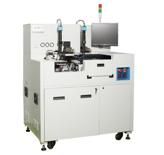
Fully Automatic Deep Cavity Wire Bonder DSP+FPGA Controller Solution
Equipment Specifications
■ Applications: Discrete devices, microwave components, lasers, optical communication devices, sensors, MEMS, SAW devices, RF modules, power devices, etc.
■ Wire Type: Gold wire (18μm-75μm)
■ Wire Loop Length, Loop Height: Fully programmable
■ Bonding Accuracy: ±3μm@3sigma
■ Ultrasonic Range: 0~0.4W control accuracy, stepped flexible application capability, adjustable in 1mW increments
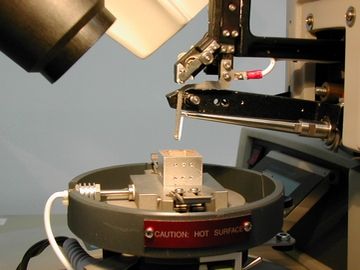
■ Cavity Depth Compatibility: ≥9mm (with 19mm capillary); ≥6mm (with 16mm capillary)
■ Pressure: 0-220g, adjustable in 1g increments
■ Compatible Capillary Lengths: 16mm, 19mm
■ Bonding Area: Large area: 304.8mmX457.2mm, 0~180° rotation range
■ Bonding Speed: ≥4wire/s
■ Operating System: Windows
■ Equipment Net Weight: 1350kg
Key Features
Real-time deformation monitoring;
Real-time ultrasonic energy monitoring;
Fixed-length, fixed-height loop control capability;
Piezoelectric ultrasonic motor tail wire control mechanism;
Deep cavity bonding capability for 16mm and 19mm capillary lengths;
High-definition bonding head maintenance image assistance tool;
Large bonding area.
C6657+Xilinx Artix-7;
C6657 + Anlogic (replacing Spartan-6);
C6657 + Tsinghua Unigroup;
All support customized development.
1 Evaluation Board Introduction Based on TI KeyStone C66x multi-core fixed-point/floating-point DSP TMS320C665x + Xilinx Artix-7 FPGA processor; The TMS320C665x has a main frequency of 1.0G/1.25GHz, with a single-core processing capability up to 40G MACS and 20G FLOPS. The FPGA XC7A100T features 101K logic cells and 240 DSP Slices; Ø The TMS320C665x and FPGA are connected via communication interfaces such as uPP, EMIF, I2C, PCIe, and SRIO, with PCIe and SRIO each supporting transmission speeds up to 5 GBaud; Ø The FPGA acquisition card supports dual-channel 250MSPS12Bit high-speed, high-precision ADCs and a single-channel 175MSPS12Bit high-speed, high-precision DAC, meeting various data acquisition requirements; It supports a Gigabit Ethernet port for connecting industrial network cameras, and also supports common interfaces such as I2C, SPI, UART, and McBSP; Ø Supports expansion modules such as CameraLink input/output and VGA output; Supports bare-metal and SYS/BIOS operating systems.
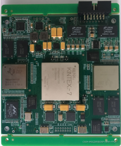 Figure 1: Physical Evaluation Board
Shenzhen Xinmai's XM-C665xF-EVM, based on TI's design, is a DSP+FPGA high-speed big data acquisition and processing architecture, suitable for high-end image processing, high-speed big data transmission, and big data acquisition and processing fields such as audio and video. This design integrates the boards via communication interfaces such as TMS320C665x's uPP, EMIF, I2C, PCIe, and SRIO, forming a DSP+FPGA architecture that delivers a unique, flexible, and powerful DSP+FPGA high-speed data acquisition and processing system.
The SOM-XM665xF brings out all CPU resource signal pins, making secondary development extremely easy. Customers only need to focus on upper-layer applications, which reduces development difficulty and time costs, enabling rapid product launch and timely capture of market opportunities. It not only provides rich demo programs but also offers DSP inter-core communication development tutorials and comprehensive technical support, assisting customers with baseboard design and debugging, as well as multi-core software development.
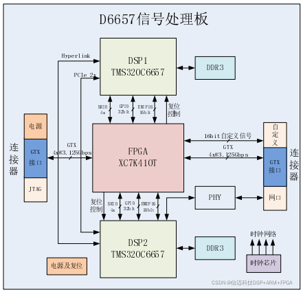
2 Typical Application Areas Data Acquisition, Processing, and Display Systems Telecom Tower: High-speed data acquisition and generation for Remote Radio Units (RRU) High-speed Data Acquisition and Processing Systems High-end Image Processing Equipment High-end Audio and Video Data Processing Communication Systems 3 Software and Hardware Parameters The front-end FPGA acquires two channels of AD data, which is then transmitted to the DSP via communication interfaces such as uPP, EMIF bus, or PCIe, SRIO interfaces. Ø After the AD data is processed by the DSP, it can be used for applications such as data comparison and analysis, network forwarding, and SATA hard disk storage. Based on the processing results, the DSP sends the derived logical control commands to the FPGA, and the FPGA controls the on-board DA to achieve logical output, with an update rate of 175MSPS.
 Figure 2: Big Data Acquisition Block Diagram
The high-speed data acquisition front-end section uses an FPGA to simultaneously acquire two channels of analog AD input signals, enabling pre-filtering of AD data, with an AD sampling rate up to 250MSPS. Another DAC channel can output parallel DA data of arbitrary amplitude and waveform, with an update rate of 175MSPS. The high-speed data transmission section consists of communication interfaces such as EMIF, I2C, PCIe, and SRIO. Large-scale throughput AD and DA data can be transmitted at high speed and stably between the DSP and FPGA via SRIO and PCIe interfaces. The DSP can perform logical control of the FPGA and exchange medium-scale throughput data via the EMIF bus, while also performing initialization settings and parameter configuration for the FPGA via I2C. (3) The high-speed data processing section consists of DSP cores and algorithm libraries. It can perform time-domain, frequency-domain, amplitude, and other signal parameters for real-time transform processing (e.g., FFT transform, FIR filtering, etc.).
(4) The video acquisition and output expansion section consists of CameraLink input/output modules, VGA output modules, Gigabit Ethernet, etc. It has rich interface resources, flexible and convenient solution selection, making it an ideal choice for high-end image processing systems.