DSP+ARM+FPGA Main Control Board Design Solution Based on C6657+ZYNQ7045
XM-6657Z45**-EVM**** Evaluation Board Specification**
Table of Contents
XM-6657Z45-EVM Evaluation Board Specification
1 Evaluation Board Introduction
3 Software and Hardware Parameters
1 Evaluation Board Introduction
- Based on TI KeyStone C66x multicore fixed-point/floating-point DSP TMS320C665x + Xilinx ZYNQ7045 FPGA processor;
- TMS320C665x has a core frequency of 1.0G/1.25GHz, with single-core processing capability up to 40G MACS and 20G FLOPS; FPGA XC7A100T has 101K logic cells and 240 DSP Slices; Ø
- TMS320C665x and FPGA are connected via communication interfaces such as uPP, EMIF, I2C, PCIe, and SRIO, with PCIe and SRIO each supporting a maximum transmission speed of 5 GBaud; Ø
- The FPGA acquisition card supports dual-channel 250MSPS*12Bit high-speed high-precision ADC, and one channel 175MSPS*12Bit high-speed high-precision DAC, meeting various data acquisition needs;
- Supports Gigabit Ethernet port, connectable to industrial network cameras, and simultaneously supports common interfaces such as I2C, SPI, UART, and McBSP; Ø
- Supports expansion modules such as CameraLink input/output and VGA output;
- Supports bare metal and SYS/BIOS operating systems.
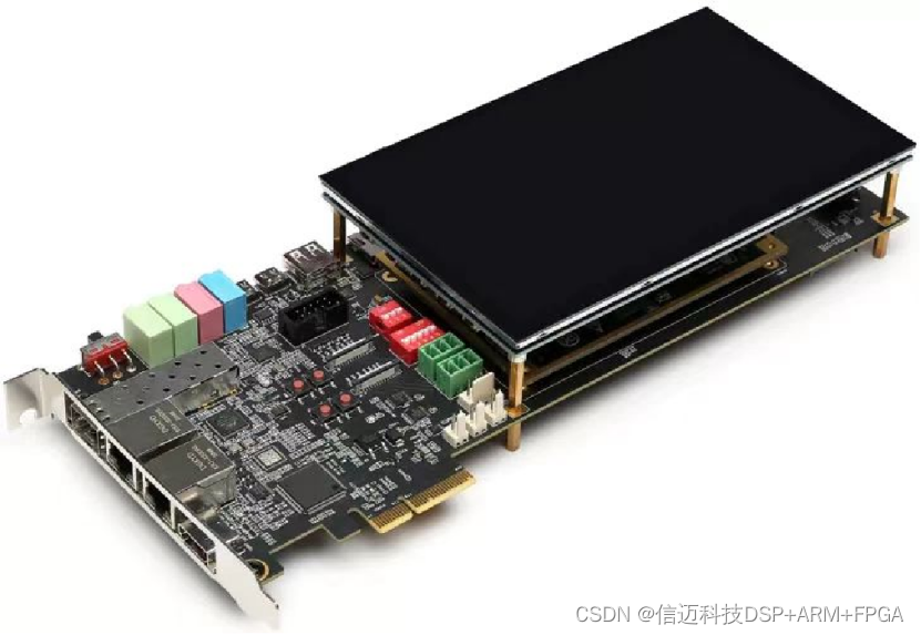
Figure 1 Actual Development Board
The XM6657-Z45-EVM, launched by Shenzhen Xinmai Technology, is a high-end heterogeneous multicore evaluation board designed based on TI C6000 series TMS320C6657 (2x C66x@1.25GHz DSP) and Xilinx Zynq-7000 series XC7Z035/XC7Z045 (2x Cortex-A9@800MHz ARM + Kintex-7 programmable logic resources) SoC processors. It consists of a core board and a baseboard.
The core board internally combines the DSP and Zynq through SPI, EMIF16, uPP, and SRIO communication interfaces, forming a DSP+Zynq architecture, thereby realizing a unique, flexible, and powerful DSP+Zynq high-speed data acquisition and processing system.
The baseboard offers rich interface resources, providing 2 bidirectional CameraLink input/output channels, 1 SFP+ optical port, 2 Gigabit Ethernet ports, dual-channel PCIe, USB, 1 4K HDMI OUT, Micro SD, LPC FMC, M.2 interface, audio input/output, and other interfaces, facilitating users to quickly conduct product solution evaluation and technical preliminary research.
The baseboard adopts an 8-layer board design with an immersion gold lead-free process, suitable for high-speed data acquisition and processing fields such as radar sonar, optoelectronic detection, underwater detection, machine vision, video communication systems, power acquisition, fiber optic cable survey instruments, medical instruments, target tracking, and rail transit.
The SOM-XM6657Z45 core board exposes all DSP and Zynq resource signal pins, making secondary development extremely easy. Customers only need to focus on upper-layer applications, which reduces development difficulty and time costs, enabling products to quickly enter the market and seize market opportunities in a timely manner.
2 Typical Application Areas
Target Recognition
Image Processing
Radar Detection
Software Defined Radio
Video Tracking
Medical Instruments
Optoelectronic Detection
Positioning and Navigation
Machine Vision
Power Acquisition
Underwater Detection
Rail Transit
3 Software and Hardware Parameters
3.1 Hardware Parameters
DSP
Processor Model: TI TMS320C6657, 2-core C66x, 1.25GHz clock frequency
Zynq
Xilinx XC7Z035/XC7Z045-2FFG676I (Optional)
2x ARM Cortex-A9, 800MHz (-2)/1GHz (-3) clock frequency, 2.5DMIPS/MHz
1x Kintex-7 architecture programmable logic resources
CPLD
MAX10 Model 10M02SCM153
FLASH
DSP SPI Flash:32MByte
FPGA SPI Flash:64MByte
EEPROM
1Mbit
DDR3
DSP DDR3:1GBytes
ZYNQ DDR3:1GBytes (PS side)
Temperature Sensor
TMP102AIDRLT
CameraLink
Supports 2 Base inputs, or 2 Base outputs, or 1 Full input or output
SFP+
1 channel supporting 10 Gigabit optical module
Gigabit Ethernet Port
DSP 1 channel
ZYNQ PS 1 channel
PCIe
1x PCIe dual-channel (DSP side)
SD
1x Micro SD
USB
1x USB 2.0
DSP IO
38
M.2
1x Connectable to SATA, 4G, 5G modules
HDMI
1x HDMI OUT (PL side)
Audio
1x LINE IN
1x MIC IN
1x LINE OUT
LPC FMC
1 channel
Power Interface
1x TYPE-C interface 12V@4A
Standard PCIe power supply
3.2 Software Parameters
Table 3
DSP Side Software Support
Bare metal, SYS/BIOS operating system
CCS Version
CCS5.5
Software Development Kit
MCSDK
Vivado Version
2015.2
4 Development Resources
(1) Provides core board pin definitions, editable baseboard schematics, editable baseboard PCB, and chip datasheets, shortening the hardware design cycle;
(2) Provides rich demo programs, including DSP multicore communication tutorials, perfectly addressing multicore development bottlenecks;
- Provides DSP and FPGA communication examples via PCIe, SRIO, I2C, etc.;
- Provides a complete platform development package and getting started tutorials, saving software organization time and making application development simpler;
Development examples mainly include: Ø
- Bare metal development examples
- SYS/BIOS development examples
- Multicore development examples
- FPGA development examples
5 Electrical Characteristics
Core Board Operating Environment
Environmental Parameters
Minimum
Typical
Maximum
Core Board Operating Temperature
-40°C
/
85°C
Core Board Operating Voltage
/
5.0V
/
Power Consumption Test
Category
Typical Voltage
Typical Current
Typical Power Consumption
Core Board
9.0v
390mA
3.5W
Note: Power consumption test is conducted based on Shenzhen Xinmai XM-6657Z45-EVM development board.
6** Mechanical Dimensions**
Table 4
Core Board
Evaluation Baseboard
PCB Dimensions
80mm*58mm
200mm*106.5mm
Number of Mounting Holes
4
4
Figure 6 Core Board Mechanical Dimensions Diagram
Figure 7 Evaluation Board Mechanical Dimensions Diagram
7 Technical Services
- Assist with baseboard design and testing to reduce hardware design errors;
- Assist in resolving abnormal issues encountered when operating according to the user manual;
- Assist with product fault diagnosis;
- Assist in correctly compiling and running the provided source code;
- Assist with product secondary development;
- Provide long-term after-sales service.
8 Value-Added Services
- Mainboard custom design
- Core board custom design
- Embedded software development
- Project cooperative development
- Technical training