ZYNQ-Based Mobile Robot Controller Design (3) Controller Hardware Selection
This chapter introduces the selection of hardware solutions for the controller. First, it answers why the ZYNQ platform was chosen for the mobile robot controller design, analyzing the inherent compatibility between ZYNQ's architecture and our proposed controller design. Then, it dedicates significant space to explaining the key technologies that will be used, assuming ZYNQ is locked in, and the overarching design methodology that should be followed throughout the application of these key technologies.
In this paper, we select Xilinx Zynq-7000 AP (All Programmable) SoC, a rising star in the embedded processor field and defined as the paradigm for next-generation embedded processors, as our implementation platform for the following reasons: (1) Superior Performance As the embedded design field continuously pursues higher performance, lower power consumption, smaller form factors, and increased flexibility, many requirements can no longer be met by existing products, including single ASICs (Application Specific Integrated Circuits), ASSPs (Application Specific Standard Products), single processors, or pure FPGA solutions, or even combinations of these. To meet the needs of next-generation application processing and respond to growing market demand, Xilinx defined the Zynq-7000 series. This series includes four new devices: 7010, 7020, 7030, and 7045. They tightly integrate ARM Cortex™-A9 multi-core processors with low-power FPGAs into a complete SoC solution. This simultaneously solves many critical problems such as insufficient signal processing capability of single processors, low reusability of ASICs, excessive size of mixed solutions combining single general-purpose processors and single FPGAs, and communication bottlenecks, bringing together high performance, low power consumption, and flexible scalability. (2) Inherent Compatibility The aforementioned advantages of ZYNQ only indicate that it is a seemingly superior processor. These advantages alone are not convincing enough to decide on it as the implementation platform for our mobile robot controller. ZYNQ's ability to outperform other processors on the market and become our optimal solution stems from the inherent compatibility between its architecture and operating mode and the robot controller we intend to design. Firstly, from an architectural perspective, ZYNQ is a heterogeneous processing platform. ZYNQ is divided into two parts: PS and PL. The PS primarily consists of a multi-core ARM Cortex A9 processor; the PL primarily consists of Xilinx's 7 Series FPGA. The two are connected via an on-chip high-speed AXI bus. In ZYNQ, the PS is the center; it can operate independently of the PL or use the PL as a peripheral or a co-processing hardware accelerator. This architecture of ZYNQ facilitates task partitioning for the controller system. We can implement control tasks suitable for general-purpose processors in software within the PS, and tasks suitable for programmable logic in hardware IP within the PL. ZYNQ's unique CPU0+CPU1+FPGA Triple Planar Architecture (TPA) allows the controller to: (1) maximize the advantages of heterogeneous multi-core processors; (2) further expand the system's optimization space; and (3) achieve better flexibility. Secondly, from an operating mode perspective, ZYNQ's unique Asymmetric Multiprocessing (AMP) system operating mode allows CPU0 and CPU1 to be configured to run their respective independent software stacks simultaneously. This operating mode enables the three-level hierarchical scheme for the mobile robot controller system, as proposed in Chapter 2 of this paper, to be realized, allowing abstract concepts to find suitable pathways and become practical systems. This is specifically shown in Figure 3-1 [18]:
In summary, ZYNQ, as an excellent processing platform, is our undisputed optimal choice in scheme selection due to its unique architecture and operating mode, which inherently align with the mobile robot controller scheme proposed in this paper, allowing it to outperform other processing chips. After locking in the ZYNQ platform, the next step is to select a development board. Among the existing Zynq-700 based development boards on the market, Xinmai Technology's ZYNQ development board ultimately caught our attention.
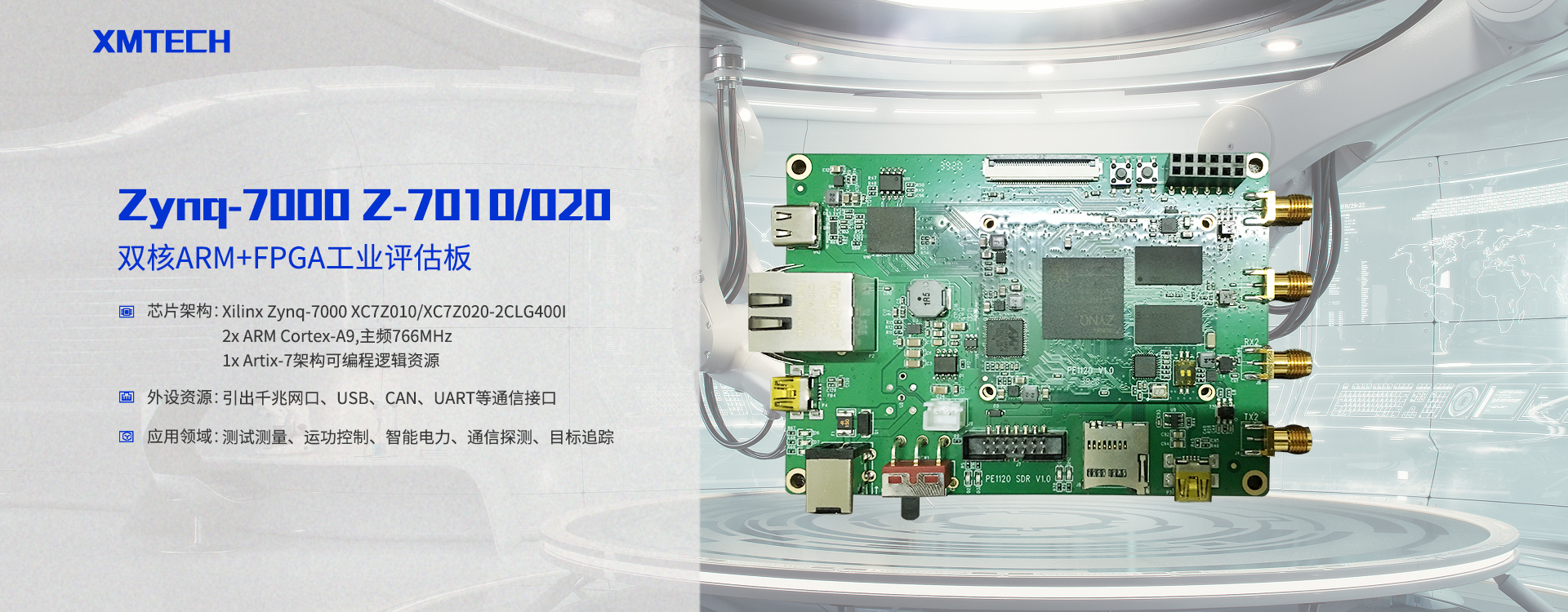
Let's briefly look at the main features and hardware resources of the XM_ZYNQ7020 as an excellent development board: Processor: ZynqTM-7000 AP SoC XC7Z020-CLG484-1 Storage: 512MB DDR; 256Mb Quad-SPI Flash; 4GB SD Card; Communication Interfaces: On-board USB-JTAG Programming port; 10/100/1000 Ethernet; USB OTG 2.0 and USB-UART ports; Expansion Interfaces: FMC-LPC connector (68 single-ended or 34 differential I/Os); 5 Pmod™ compatible headers (2x6); Agile Mixed Signaling (AMS) header;
Clock: 33.33333MHz PS clock source; 100MHz PL crystal oscillator; Display: HDMI output (1080p60 with 16-bit, YCbCr, 4:2:2 mode color); VGA output (12-bit resolution color); 128*32 OLED display; Configuration and Debugging: On-board USB-JTAG interface; Xilinx Platform Cable JTAG port; General-purpose I/O: 8 user LEDs; 7 push buttons; 8 DIP switches; Concepts such as PS (Processing System), PL (Programmable Logic), and EMIO will be introduced in more detail later in this chapter. 3.1 Key Technologies of ZYNQ The main chip used by Zedboard, Zynq, is fully named Zynq AP SoC, which stands for Zynq All Programmable SoC. It is defined by Xilinx as a next-generation embedded processor, possessing many new features not found in any previous embedded processor. Therefore, this paper needs to dedicate some space to presenting and summarizing them. This section mainly introduces the ARM+FPGA architecture, operating modes, and interface technologies of the Zynq AP SoC platform. As shown in Figure 3-3, the top-left block is the ARM part, which we refer to as the Processing System (PS) in the Zynq AP SoC platform. The part enclosing the PS is the FPGA, which we refer to as Programmable Logic (PL).
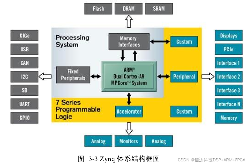
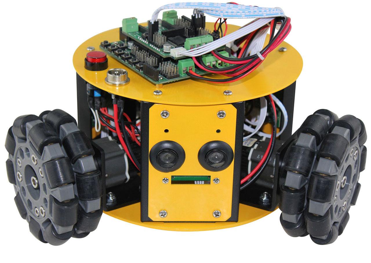
The Zynq-7000 architecture has distinct highlights and advantages that differentiate it from any previous multi-chip solution or pure FPGA solution. It includes a complete ARM processing subsystem, with this subsystem at the core of ZYNQ. Even without the FPGA, the processing subsystem can operate independently, relying on its integrated memory controller and numerous peripherals. This is a feature not found in any previous FPGA processor [20]. Under this premise, the programmable logic part is tightly integrated with the ARM processing unit through dedicated bus devices, forming a seamless whole. In addition to the high-performance ARM Cortex™-A series CPU, the Zynq AP SoC platform excellently integrates Xilinx 7 Series FPGAs, which utilize an extremely advanced 28nm process. Among them, the Z-7010 and Z-7020 target low-end applications, using Xilinx Artix-7, while the Z-7030 and Z-7045 target high-end applications, using Xilinx Kintex-7. The FPGA in the PL part of the Zynq-700 AP SoC is used to expand the subsystem. It has powerful scalability, supporting over 3000 internal interconnections, offering very rich connection resources, and providing internal bandwidth exceeding 100Gb/s. Furthermore, in terms of I/O interfaces, users can fully customize them. In addition, the FPGA part integrates high-speed serial ports (Multi Gigabit Transceiver) and digital-to-analog converters (XDC). The Xinmai XM_ZYNQ7020 development board selected in this paper uses the Z-7020 chip. Next, we will provide a relatively detailed introduction to the technical details and parameters of the application processing unit, general-purpose peripherals, and digital logic design parts of Zynq that are relevant to this design. Other parts not involved in the design scheme will be omitted for brevity.
3.1.1 Processing System The ZYNQ architecture is divided into the Processing System (PS) and Programmable Logic (PL). The Application Processing Unit (APU) introduced in this section is located on the PS side. Its detailed architectural details are shown in Figure 3-4 below:
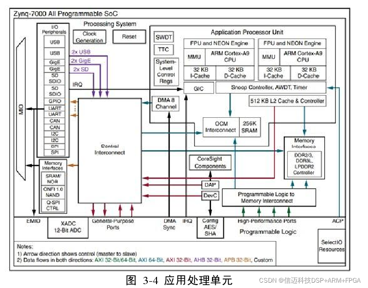
The APU contains two ARM Cortex™-A9 processors and two Neon co-processors, which share a 512KB L2 cache. Each processor has a high-performance, low-power core and independently possesses 32KB of L1 instruction and data cache. The ARM Cortex™-A9 is a processor based on the ARMv7-A architecture, supporting virtual memory, and can currently execute 32-bit ARM instructions, 16 and 32-bit Thumb instructions, and 8-bit Java™ bytecode in Jazelle state. The Neon co-processor's media and signal processing architecture enhances audio, video, image, and speech processing capabilities, and even includes targeted instruction optimization for 3D graphics. These advanced Single Instruction Multiple Data (SIMD) instructions can be executed in both ARM and Thumb states. For brevity, this paper will only elaborate on the unique aspects of the APU, and will not delve into the technical details specific to Cortex™-A9. (1) Snoop Control Unit The Snoop Control Unit (SCU) module is a major feature of the Zynq-7000 Application Processing Unit. It connects to the two Cortex™-A9 processors and their memory subsystems. It is used to ensure consistency between the two processors and with the ACP interface from the PL. It intelligently manages data consistency between the two processors and the shared L2 cache. This module is responsible for managing interconnect arbitration, communication, caching, transfers between system memory, and data consistency between caches for the processors. Additionally, the APU provides a system accelerator implemented in the PL, which connects to the SCU module via the Accelerator Coherence Port (ACP). This interface allows the PL to share and access the processor's caches. Such system consistency management provided by an independent hardware management unit not only improves performance but also reduces software complexity, with the greatest advantage being the maintenance of driver consistency across different operating systems.
The SCU module communicates with each Cortex™-A9 processor via the Cache Coherency Bus (CCB). The SCU supports MESI (Modified, Exclusive, Shared, Invalid) snooping, achieving higher efficiency and performance by avoiding unnecessary system accesses. The SCU module implements a 4-way associative RAM tag as a local directory in the L1 data cache to check data relevance. This directory allows the SCU module to check if data is in the L1 cache at extremely high speed without interrupting the processor. Furthermore, the SCU module can filter accesses to the processor providing shared data. The SCU module can also copy "clean" data from one processor's cache to another processor's cache without involving main memory in the process. Additionally, it can move "dirty" data between processors while avoiding the latency caused by shared write-back operations. For example: when a processor writes to memory, it only writes to the cache, not to main memory. If a second A9 performs a read operation that involves a data segment dirtied by the first write, the SCU must ensure that the second A9's cache contains the latest data. If the second A9 writes data to the same data segment, the content of the write needs to be reflected in the first. The existence of the SCU is what makes the two cores interconnected "dual cores" and enables them to be an MPSoC (Multi Processor System on Chip). In the scheme adopted in this paper, CPU0 and CPU1 communicate via shared OCM. Since shared resources are involved, there must be corresponding measures to prevent conflicts that may arise during resource sharing. When planning the strategy for this part, the author used the SCU to impose relevant restrictions on the OCM's corresponding caches. Specifically, CPU0 starts first, and its Linux system disables flushing via L2. CPU1, when logically started, also performs similar restrictions in its BSP. See Chapter 5 of the paper for details. (2) APU Interfaces The APU is the most critical component in the system; it connects the PS, IPs implemented in the PL, external access devices, and board-level devices such as peripherals. As shown in the figure above, the APU communicates with the rest of the system through two interfaces of the L2 controller and one interface to the OCM (OCM and L2 cache are parallel). Within the APU, there are two most important types of interfaces: one is the common interrupt interface found in processors, and the other is the Zynq-7000's very unique Accelerator Coherence Port, through which the FPGA in the PL can achieve hardware acceleration for the APU. The position of the ACP interface in the APU is shown in the upper left of the figure above. Here, we will briefly introduce this relatively special interface: The Accelerator Coherence Port (ACP) is a 64-bit slave interface. It is a port that:
- Provides an asynchronous cache-coherent access point, directly accessible from the PL to the SCU of the Cortex™-A9 MP-core processor. The PL can use this interface to access the entire APU's cache and memory system, thereby simplifying software implementation and improving system performance.
- This interface acts as a standard AXI slave device, supporting all standard read and write operations without needing to add any Programmable Logic components.
- This is a lower-latency path between the PL-side accelerator and the PS-side compared to traditional Cache flushing and Cache loading. The ZYNQ chip's memory system is a common multi-level memory system, which the author will not elaborate on here. However, the access operations to the memory system also highlight ZYNQ's uniqueness, as briefly mentioned in the SCU introduction above. The ACP interface is no exception; observing the internal module connection diagram of the APU above, the ACP interface is also connected to various levels of storage devices through the SCU module. In fact, any operation to read a contiguous memory block via the ACP interface cannot bypass the SCU module but must go through the following logic: the SCU module checks if the required information is already stored in the L1 cache (32KB size). If it exists, it's a hit, and the data will be returned directly; if it's a miss, meaning the data is not in the L1 cache, there is still a chance for a hit in the next-level L2 cache (512KB size). If neither hits, it will eventually be forwarded to main memory. For write operations performed via the ACP interface, when writing to a contiguous memory region, the SCU maintains coherence before the write is transferred to the memory system. Write operations can be selectively placed in the L2 cache to reduce the impact of increased power consumption and decreased performance caused by unnecessary writes to off-chip memory. Regarding the other type of interface in the APU: the interrupt interface, given that it is not significantly different from common processor interrupt ports, this paper will not elaborate further due to space constraints. 3.1.2 ZYNQ's Programmable Logic In fact, before the Zynq-7000, the demand for combining high-performance general-purpose processors with large-scale reconfigurable devices like FPGAs had already emerged. On one hand, the reconfigurable capabilities of FPGAs can provide ASIC-comparable performance in many fields, especially signal processing. On the other hand, general-purpose processor technology is mature, not only offering rich control functions but also being easy to program using C language. The combination of the two allows applications to be partitioned based on what the CPU and FPGA excel at, thereby achieving desired development outcomes while leveraging their respective advantages. However, before ZYNQ appeared, the two could only be combined off-chip, meaning the CPU would offload computationally intensive parts to the FPGA for implementation, with the two connected via some off-chip interface for data exchange, unable to form a System on Chip. As discussed earlier, ZYNQ successfully integrates high-performance general-purpose processors and FPGAs into a single System on Chip, eliminating communication bottlenecks. A new hybrid architecture for SoCs has emerged. This opens up many new possibilities for embedded development. In this hybrid architecture, the general-purpose processor supports running a standard operating system, meaning existing software can be seamlessly ported to one of ZYNQ's cores for convenient programming and interaction. At the same time, the presence of Programmable Logic provides more flexible user interfaces. When a program involves a large number of parallel behaviors or serial behaviors that can be converted to parallel, implementing that part on an FPGA is ideal. This subsection introduces the key aspects of Programmable Logic relevant to this paper, including PL resource characteristics, the role and use cases of PL in ZYNQ, and ZYNQ's unique "Planar Pattern" adopted by the mobile robot controller solution implemented in this paper. Programmable Logic Resource Characteristics Each device in the Zynq-7000 series contains the same PS, but the PL and I/O resources within each device differ. The PL of the two smaller capacity devices, Z-7010 and Z-7020, is based on Artix-7 FPGA, while the PL of the two larger capacity devices, Z-7030 and Z-7045, is based on Kintex-7 FPGA. Through multiple interfaces and over 3000 central interconnect structures, the PL and PS can be loosely or tightly coupled. Hardware accelerators created within the PL can be efficiently integrated with other functions; processors can access them, and they can also access memory resources within the PS. ZYNQ always starts the general-purpose processor located in the PS first (usually CPU0), and then configures the PL using a bitstream. PL configuration can be part of system startup or configured at a later stage, either fully reconfigured or dynamically partially reconfigured (Partial Reconfiguration, PR) when in use, for example, to update coefficients or replace algorithms to time-share PL resources. The latter is similar to dynamically loading and unloading modules in software development. The PL configuration data is a bitstream file, represented by files with a .bit extension. The PL provides rich resources that users can flexibly configure. Here, we will only introduce the configurable logic blocks (CLB), 36Kb block RAM, etc., which are unique ZYNQ resources and relevant to this paper.
- CLB, Slice, and LUT CLB, Slice, and LUT are unique concepts in FPGAs and are often used as performance indicators to measure how many resources a program consumes.
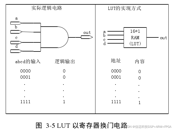
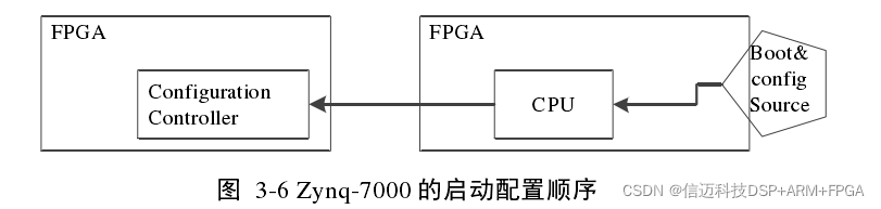
A LUT is the smallest unit of programmable logic in an FPGA. Figure 3-5 shows the schematic of a LUT using memory to implement logic gates. The LUTs in Zynq-7000 can be configured as a 6-input LUT with 1 output (64-bit ROM) or two 5-input LUTs with independent outputs and common address/logic inputs (32-bit ROM). A Slice consists of 4 such LUTs, 8 flip-flops, multiplexers, and arithmetic carry logic. Two Slices form a CLB. The number of LUTs and CLBs consumed in a design is often used to measure whether the program is concise and efficient. 2) Block RAM Block RAM, also known as BRAM, is another concept unique to FPGAs. Each Zynq-7000 has 60 to 465 BRAMs, each with a capacity of 36Kb. Each BRAM has two independent ports. Its key features include: (1) Dual-port (2) Maximum 72-bit width (3) Configurable as dual 18Kb (4) Programmable FIFO logic and built-in FIFO logic PL's Role and Use Cases in ZYNQ's Hybrid Architecture This section introduces the role and use cases of PL in ZYNQ's hybrid architecture. In Zynq-7000, the PL always starts after the PS, and the PS uses a bitstream file to configure the PL. As shown in Figure 3-6, this differs from its competitor, Altera's competing product, which is also a hybrid FPGA/CPU solution. In the latter, the CPU and FPGA do not have a strict startup order; the FPGA can start and configure after the CPU, or before the CPU, or even the FPGA and CPU can start and configure independently [18].
Based on the functional role of PL in Zynq, common use cases for PL primarily fall into three types, as shown in Figures 3-7A, B, and C:
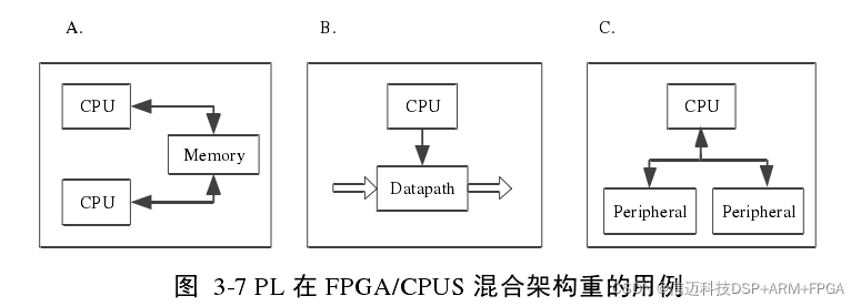
Figure A shows a combination of PL and PS [18], where the FPGA acts as a hardware accelerator for the general-purpose processor. In this scenario, computationally intensive operations (often highly parallel behaviors or serial behaviors that can be converted to parallel) are allocated to the Programmable Logic (PL) to improve system performance. Common applications include designing and placing DSP logic in the PL. In addition to designing dedicated logic in the PL for hardware acceleration, the PL can also be used as a servo subsystem. Figure B shows another combination of PL and PS [18], where real-time tasks are executed in the PL, and non-real-time tasks are executed in the PS. This allocation strategy builds a ZYNQ-unique "multi-faceted structure" where high-speed and low-speed paths coexist. For example, when developing network applications, the high-speed path handles packet forwarding, and the low-speed path handles some control functions. In such cases, this "multi-faceted structure" is very suitable. Besides the two use cases mentioned above, there are other situations. Figure C above shows a third possibility for combining PL and PS [18]. In this case, the PL is used to extend the PS's peripheral interfaces. If some interfaces are resource-constrained in the PS and cannot be accommodated, they can be brought out for user use by adding corresponding IPs in the PL. Since FPGAs have abundant gate resources (Z-7020 has approximately 1.3 million gates), this greatly expands the PS's interface capabilities. We can add common peripherals such as UART, IIC, CAN, USB, Ethernet, etc. In this paper, CPU1 sends action commands to Arduino to drive motors and enable robot movement, which is achieved by adding a Uart_lite IP core in the PL. 3.1.3 ZYNQ's Operating Modes As discussed in the previous section on PL's second use case in ZYNQ's FPGA/CPUs hybrid architecture, the CPU and FPGA can be seamlessly connected as two subsystems. Since each excels in different areas, we can optimize performance by reasonably partitioning applications, placing tasks suitable for the CPU in the PS and tasks suitable for the FPGA in the PL. This section details ZYNQ's unique Triple Planar Architecture (TPA), which is the scheme we adopted for implementing our mobile robot controller. As shown in Figure 3-8, Xinmai Technology's XM_ZYNQ7020 provides us with a platform: a hybrid architecture of a dual-core ARM Cortex™-A9 processor + 7 Series FPGA. Such an architecture can be divided into three "planes," a division known as "Triple Planar Architecture" (TPA). To implement such an architecture, the CPU must be configured as an Asymmetric Multiprocessing system (AMP) [18], rather than a Symmetric Multiprocessing system (SMP). In AMP mode, each CPU core can independently run a different operating system to suit different needs. For example, a real-time operating system (RTOS) can be run on the "plane" responsible for real-time tasks. AMP mode is typically used in communication/remote control systems, where one CPU core can be used to control information channels and process acquired information, while the remaining CPU cores can be responsible for implementing high-performance requirements, such as packet forwarding.
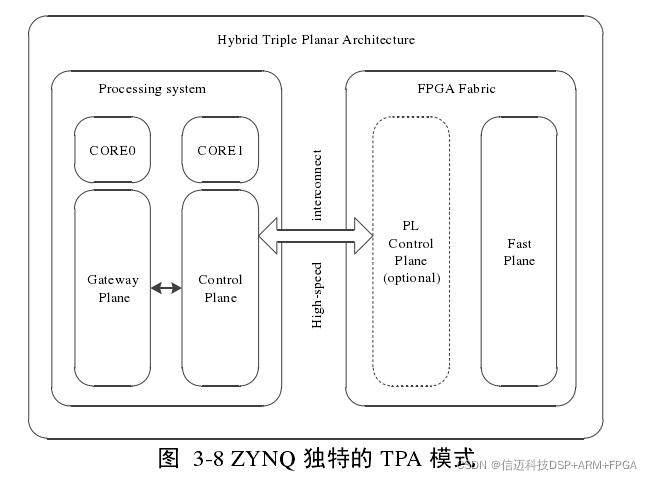
In this "Triple Planar Architecture," one CPU core is responsible for interacting with the user (the Gateway Plane in the figure) to receive user commands, and another CPU core is used to receive information from the Fast Plane and send commands to it. This describes a scenario where sensors in the Fast Plane acquire data. After acquiring sensor data, it is first sent to the Control Plane, where data format conversion is completed, and then sent to the Gateway Plane to be displayed to the user. The Gateway Plane then converts the data into a format suitable for communication (e.g., Ethernet). If the PL also needs to implement control or scheduling-intensive tasks, soft cores such as the famous MicroBlaze and Nios II can be optionally added to the FPGA, depending on actual requirements. This paper, in implementing its mobile robot controller, utilizes this "Triple Planar Architecture." In our system, CPU0 is responsible for high-performance tasks such as human-machine interaction, running a Linux operating system. It receives data information from CPU1 and forwards it to the control interface via HTTP protocol, allowing users to monitor the robot's current status and manually issue action commands to the robot, equivalent to the Gateway Plane in the figure above, which is the interaction layer in the system's three-layer structure. CPU1 is responsible for real-time tasks, equivalent to the Control Plane in the figure above. It obtains sensor information from the Fast Plane, converts its format, and forwards it to CPU0, while also sending action commands to the drivers, corresponding to the real-time control layer in the system's three-layer structure. Logic responsible for triggering and scheduling 8-16 ultrasonic sensors is created in the PL. The PL sends the acquired real-time sensor data to CPU1 via the AXI interface, equivalent to the Fast Plane in the figure above, corresponding to the drive and sensing layer in the system's three-layer structure.